 ChipApex | Global Electronic Components Supplier
74LVC827APW,112
Search Product
Search Post
— IC芯片 | 连接器 | 传感器 | 被动器件 —
Search productSearch post
— IC芯片 | 连接器 | 传感器 | 被动器件 —
Consult the customer manager about the wholesale price.
consultation hotline:86-132-6715-2157
email:[email protected]
Contact the product manager for consultation. One-stop consultation is available.
Do you want a lower wholesale price? Please send us your inquiry and we will reply immediately.
The Nexperia 74LVC827APW,112 is a 10-bit buffer and line driver featuring 3-state outputs controlled by OE1 and OE2 pins. It operates within a supply voltage range of 1.2 V to 3.6 V and supports inputs driven from 3.3 V or 5 V devices. The device provides 5 V tolerant inputs and outputs for interfacing with 5 V logic. It complies with JEDEC standards JESD8-7A, JESD8-5A, and JESD8-C/JESD36. ESD protection exceeds 2000 V (HBM), 200 V (MM), and 1000 V (CDM). Operating temperature ranges from -40 °C to +125 °C.
Verify the specific ordering suffix '112' corresponds to the TSSOP24 package (SOT355-1) as defined in the official Nexperia datasheet. Confirm that the required operating temperature range of -40 °C to +125 °C aligns with your application environment. Ensure input and output voltage levels remain within the specified 5 V tolerance limits to prevent damage.
Select this component when a 10-bit bidirectional buffer with 3-state capability is required for mixed-voltage environments. It is suitable for designs needing direct interface with TTL levels and compliance with specific JEDEC standards. Consider the TSSOP24 package constraints regarding body width and lead pitch during PCB layout planning.
This part belongs to the Nexperia LVC logic family, designed for low-voltage CMOS applications. The 74LVC827A series specifically addresses the need for high-density buffering in portable and battery-powered devices. It serves as a bridge between different logic voltage domains while maintaining signal integrity through controlled drive strengths and 3-state functionality.
Check for equivalent parts such as the 74LVC827AD or 74LVC827ADB if alternative packages like SO24 or SSOP24 are acceptable. Verify pin compatibility and electrical specifications before substitution.
The outputs enter a high-impedance OFF-state when either OE1 or OE2 input pins are driven HIGH. They assume the state of the data inputs when the respective enable pin is LOW.
Yes, the 74LVC827APW,112 features 5 V tolerant inputs and outputs, allowing it to be used as a translator in mixed 3.3 V and 5 V applications.
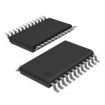 74LVC827APW,112
The activity of extra discounts on wholesale prices is in full swing…
Please fill in your contact information and we will send you the latest wholesale price list.





