 ChipApex | Global Electronic Components Supplier
SEARCH
Search Product
Search Post
— IC芯片 | 连接器 | 传感器 | 被动器件 —
Search productSearch post
— IC芯片 | 连接器 | 传感器 | 被动器件 —
Consult the customer manager about the wholesale price.
consultation hotline:86-132-6715-2157
email:[email protected]
Contact the product manager for consultation. One-stop consultation is available.
Do you want a lower wholesale price? Please send us your inquiry and we will reply immediately.
The NXP USA Inc. 74LVCH162374ADGG:5 is a dual 8-bit D-type edge-triggered flip-flop housed in a TSSOP-48 (SOT-362) package. It operates within a supply voltage range of 1.2 V to 3.6 V, supporting 5 V tolerant I/O for mixed-voltage interfacing. The device features single-ended non-inverting inputs and outputs with a propagation delay of 3.8 ns at 3.3 V. It provides high-level output current capability of -12 mA and functions reliably across an extended temperature range from -40 °C to +125 °C.
Verify the specific ordering suffix ':5' against official NXP documentation to confirm exact packaging configuration and reel specifications. Ensure compatibility with required thermal management standards for the SOT-362 package. Confirm RoHS compliance status and lead-free soldering requirements prior to integration into manufacturing processes.
Select this component when designing systems requiring dual 8-bit edge-triggered storage with 5 V tolerance. The LVCH series offers low inductance supply pins to minimize noise. Verify that the 3.8 ns propagation delay meets system timing constraints and that the -40 °C to +125 °C operating range satisfies environmental conditions.
This part belongs to the NXP 74LVCH series, designed for low-voltage CMOS applications. It complements other bus drivers and transceivers in the LVC/LCX/Z family. The TSSOP-48 package allows for compact surface-mount assembly. It serves as a critical component for data retention in complex digital logic designs requiring reliable edge-triggered functionality.
Public confirmed substitute part numbers include 74LVCH162374ADG and 74LVCH162374ADGG,5. Verify pinout compatibility and electrical parameter equivalence before substitution. Ensure the alternative part number matches the required TSSOP-48 package and 5 V tolerant specifications.
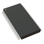 74LVCH162374ADGG:5
The activity of extra discounts on wholesale prices is in full swing…
Please fill in your contact information and we will send you the latest wholesale price list.





