ChipApex | Global Electronic Components Supplier
74LVCH16244ADGG,112
Search Product
Search Post
— IC芯片 | 连接器 | 传感器 | 被动器件 —
Search productSearch post
— IC芯片 | 连接器 | 传感器 | 被动器件 —
Consult the customer manager about the wholesale price.
consultation hotline:86-132-6715-2157
email:[email protected]
Contact the product manager for consultation. One-stop consultation is available.
Do you want a lower wholesale price? Please send us your inquiry and we will reply immediately.
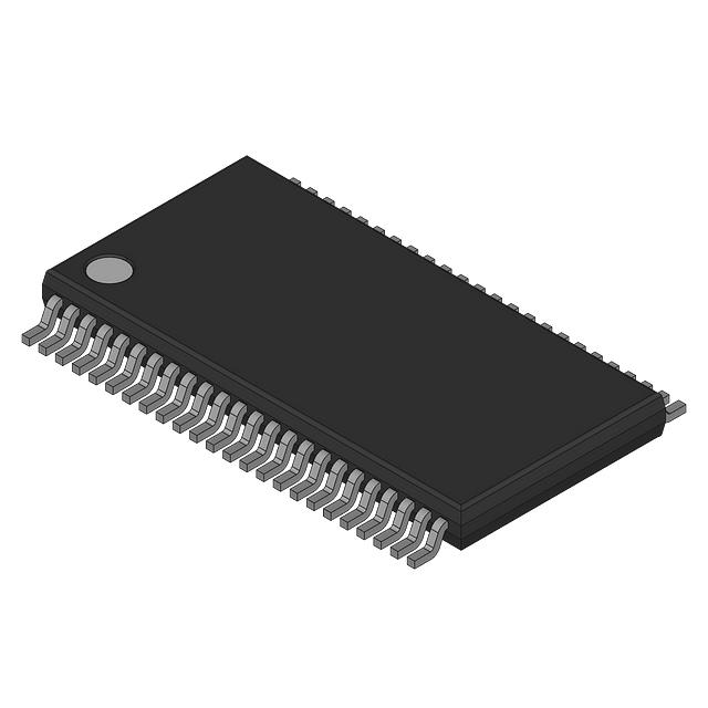
The Nexperia 74LVCH16244ADGG,112 is a 16-bit buffer and line driver featuring three-state outputs. It operates within a supply voltage range of 1.2 V to 3.6 V and provides input/output tolerance up to 5.5 V for interfacing with 5 V logic systems. The device includes four independent output enable inputs (1OE, 2OE, 3OE, 4OE) controlling groups of four outputs each. Data inputs incorporate bus hold circuitry to maintain stable states without external pull-up resistors. The component utilizes an IOFF feature to prevent backflow current during partial power-down conditions.
Verify the specific ordering suffix matches the required package variant. Confirm the temperature range specification aligns with the intended operational environment. Ensure the design accounts for the low-inductance multiple power and ground pin architecture to minimize noise and ground bounce effects during high-speed switching operations.
Select this component when a 16-bit buffer requires compatibility with 5 V logic levels while operating from lower supply voltages. The inclusion of bus hold circuits simplifies board layout by removing the need for external pull-up components on unused or floating inputs. Verify that the application benefits from the specified ESD protection ratings and low power consumption characteristics inherent to the CMOS technology.
This part belongs to the 74LVC/LVCH16244A family of 16-bit buffers and line drivers. It shares functional similarities with the standard 74LVC16244A but adds specific features such as bus hold on data inputs. The ADGG suffix indicates a TSSOP48 plastic thin shrink small outline package with a body width of 6.1 mm, designed for surface-mount assembly.
The 74LVC16244ADGG,112 serves as a compatible alternative to the 74LVCH16244ADGG,112. Both devices share identical pinouts and core functionalities within the same package configuration.
The integrated IOFF circuitry automatically disables the outputs to prevent potentially damaging backflow current through the device when it is in a partial power-down state.
The bus hold circuitry maintains the logic state of the data inputs, which eliminates the need for external pull-up resistors to hold unused inputs at a defined level.
Yes, the inputs and outputs are tolerant up to 5.5 V, allowing direct interfacing with 5 V logic devices even when the device itself operates at lower supply voltages.
 74LVCH16244ADGG,112
The activity of extra discounts on wholesale prices is in full swing…
Please fill in your contact information and we will send you the latest wholesale price list.