 ChipApex | Global Electronic Components Supplier
74LVCH16245ADGGRG4
Search Product
Search Post
— IC芯片 | 连接器 | 传感器 | 被动器件 —
Search productSearch post
— IC芯片 | 连接器 | 传感器 | 被动器件 —
Consult the customer manager about the wholesale price.
consultation hotline:86-132-6715-2157
email:[email protected]
Contact the product manager for consultation. One-stop consultation is available.
Do you want a lower wholesale price? Please send us your inquiry and we will reply immediately.
The SN74LVCH16245A is a 16-bit (dual-octal) noninverting bus transceiver designed for asynchronous communication between data buses. It operates from a supply voltage range of 1.65 V to 3.6 V and features inputs that accept voltages up to 5.5 V, supporting mixed-mode signal operation in 5-V input/output environments with 3.3-V VCC. The device provides a maximum propagation delay of 4 ns at 3.3 V and includes active bus-hold circuitry on data inputs to maintain valid logic states without external resistors. It supports partial-power-down mode via Ioff circuitry and offers ESD protection exceeding 2000 V per the human-body model.
Verify the specific package variant against the orderable addendum, as the DGGRG4 designation corresponds to the TSSOP-48 package. Confirm RoHS compliance and lead finish specifications (NIPDAU) match the design requirements. Ensure the operating temperature range of -40°C to +125°C aligns with the environmental conditions of the target application.
Select this component when interfacing buses with different voltage levels, specifically translating between 5-V tolerant systems and 1.65-V to 3.6-V logic domains. The dual-octal architecture allows configuration as two independent 8-bit transceivers or a single 16-bit unit. Consider the 4-ns propagation delay and drive capabilities for high-speed data paths requiring low skew and balanced output drive.
This device belongs to Texas Instruments' Widebus Family, which specializes in wide-bus transceivers for parallel data transmission. The SN74LVCH16245A utilizes CMOS technology to achieve balanced output drive characteristics. It is part of the LVCH series, distinguished by its ability to tolerate 5-V inputs across the entire 1.65-V to 3.6-V supply range, facilitating integration in multi-power system environments.
SN74LVC16245ADGGRG4
The SN74LVCH16245A incorporates active bus-hold circuitry that holds unused or undriven data inputs at a valid logic state. This internal feature eliminates the requirement for external pullup or pulldown resistors.
The Ioff circuitry supports partial-power-down mode by disabling the outputs when VCC is 0 V. This prevents damaging current backflow through the device when it is powered down but the system remains energized.
Yes, the device allows down voltage translation. Its inputs accept voltages up to 5.5 V regardless of the VCC level, enabling use as translators in mixed 3.3-V and 5-V system environments.
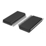 74LVCH16245ADGGRG4
The activity of extra discounts on wholesale prices is in full swing…
Please fill in your contact information and we will send you the latest wholesale price list.





