 ChipApex | Global Electronic Components Supplier
74LVCH16541ADGG,51
Search Product
Search Post
— IC芯片 | 连接器 | 传感器 | 被动器件 —
Search productSearch post
— IC芯片 | 连接器 | 传感器 | 被动器件 —
Consult the customer manager about the wholesale price.
consultation hotline:86-132-6715-2157
email:[email protected]
Contact the product manager for consultation. One-stop consultation is available.
Do you want a lower wholesale price? Please send us your inquiry and we will reply immediately.
The Nexperia 74LVCH16541ADGG is a 16-bit buffer and line driver featuring three-state outputs controlled by dedicated enable inputs. It operates within a supply voltage range of 1.2 V to 3.6 V, supporting CMOS low-power consumption. The device incorporates bus hold circuitry on all data inputs to eliminate the need for external pull-up resistors. It provides high-impedance outputs when powered down and ensures compatibility with mixed 3.3 V and 5 V logic environments.
Verify the specific ordering suffix against official Nexperia documentation to confirm package type and temperature rating. Ensure the procurement channel sources directly from authorized distributors to guarantee component authenticity and adherence to current JEDEC standards.
Select this component for designs requiring wide supply voltage flexibility between 1.2 V and 3.6 V. The integrated bus hold feature simplifies PCB layout by removing the requirement for external pull-up resistors on unused or floating input lines.
This device belongs to the LVCH logic family, designed for low-voltage CMOS applications. It utilizes a standard multibyte flow-through pin-out architecture, facilitating easy integration into existing digital circuit topologies that require parallel data buffering.
Consult official Nexperia substitution guides for verified equivalents. Cross-referencing requires matching the TSSOP48 package (SOT362-1) and ensuring identical electrical characteristics for the target application environment.
All data inputs are equipped with bus hold circuits, which automatically hold the input at a defined logic level, eliminating the need for external pull-up or pull-down resistors.
When VCC is 0 V, the outputs assume a high-impedance OFF-state, preventing damaging backflow currents through the device in partial power-down scenarios.
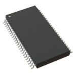 74LVCH16541ADGG,51
The activity of extra discounts on wholesale prices is in full swing…
Please fill in your contact information and we will send you the latest wholesale price list.





