 ChipApex | Global Electronic Components Supplier

SEARCH
Search Product
Search Post
— IC芯片 | 连接器 | 传感器 | 被动器件 —
Search productSearch post
— IC芯片 | 连接器 | 传感器 | 被动器件 —
Consult the customer manager about the wholesale price.
consultation hotline:86-132-6715-2157
email:[email protected]
Contact the product manager for consultation. One-stop consultation is available.
Do you want a lower wholesale price? Please send us your inquiry and we will reply immediately.
74LVXC4245WM is listed in the Translators, Level Shifters range at ChipApex. The manufacturer field lists onsemi. Its product description is IC TXRX NON-INVERT 5.5V 24SOP. Review the specifications below when checking this part for your BOM.
The onsemi 74LVXC4245WM is an 8-bit dual-supply configurable voltage interface transceiver with 3-STATE outputs. It operates with a fixed VCCA of 4.5V to 5.5V and a flexible VCCB range of 2.7V to 5.5V. The device provides bidirectional data transfer between the A and B ports, controlled by OE and T/R inputs. It features TTL-compatible control inputs and outputs capable of sourcing or sinking up to 24 mA. Propagation delays typically range from 1.0 ns to 8.0 ns depending on supply conditions. The component is housed in a 24-lead SOIC package.
Verify the specific ordering suffix to confirm the package type, as the base part number may correspond to different physical packages such as SOIC, QSOP, or TSSOP. Confirm that the VCCA supply is strictly maintained at 5V levels, as this is required for internal references. Ensure unused A port pins are tied to valid logic levels during operation to prevent floating states. Check current availability status as distribution channels may vary.
Select this component when a dual-supply translator is required to bridge 5V systems with variable 3V-to-5V peripherals. It is specifically suited for applications where the peripheral voltage rail may change or float, such as PCMCIA sockets. Ensure the design can accommodate the requirement for VCCA to be powered before VCCB to prevent bus contention during power-up sequences.
This device belongs to the LVXC family of low-voltage CMOS transceivers designed for dual-supply operations. It serves as a bridge between different voltage domains within a single system. The 'WM' suffix specifically denotes the 24-Lead Small Outline Integrated Circuit (SOIC) package variant manufactured under the Fairchild Semiconductor lineage now integrated into ON Semiconductor.
SN74LVCC4245ADWR
Yes, the device allows the B Port and VCCB pin to float simultaneously when the Output Enable (OE) input is HIGH. This feature is necessary for applications like PCMCIA sockets that permit card insertion and removal during normal operation.
To prevent bus contention, VCCA must be powered up first. The OE and T/R control pins should ramp with or ahead of VCCA. Unused A side data inputs must be driven to a valid logic level to prevent excessive current draw.
Explore related parts through Logic, Integrated Circuits (ICs), all product categories, ChipApex homepage.
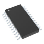 74LVXC4245WM

The activity of extra discounts on wholesale prices is in full swing…
Please fill in your contact information and we will send you the latest wholesale price list.





