 ChipApex | Global Electronic Components Supplier

SEARCH
Search Product
Search Post
— IC芯片 | 连接器 | 传感器 | 被动器件 —
Search productSearch post
— IC芯片 | 连接器 | 传感器 | 被动器件 —
Consult the customer manager about the wholesale price.
consultation hotline:86-132-6715-2157
email:[email protected]
Contact the product manager for consultation. One-stop consultation is available.
Do you want a lower wholesale price? Please send us your inquiry and we will reply immediately.
74SSTUB32865AZJBR is listed in the Specialty Logic range at ChipApex. The manufacturer field lists Texas Instruments. Its product description is IC REGSTR BUFF 28-56BIT 160NFBGA. Review the specifications below when checking this part for your BOM.
The Texas Instruments 74SSTUB32865AZJBR is a 28-bit to 56-bit registered buffer with address-parity test, designed for 1.7V to 1.9V VCC operation. It supports SSTL_18 data inputs and LVCMOS switching levels on chip-select gate-enable and RESET inputs. The device features differential clock (CK and CK) inputs, with data registered at the crossing of CK going high and CK going low. It includes an open-drain error (PTYERR) output that indicates parity errors on DIMM-independent data inputs. The component operates within an industrial temperature range of -40°C to 85°C.
Verify component authenticity through authorized distributors or direct manufacturer channels. Confirm the specific ordering suffix matches the required package and tape-and-reel specifications. Ensure compliance with RoHS3 standards and check for any product change notices affecting availability or assembly sites. Validate that the part number corresponds to the exact 160-NFBGA configuration required for the design.
Select this component for designs requiring a 28-bit to 56-bit registered buffer with address-parity testing capabilities. It is suitable for applications needing high driver strength for heavily loaded DIMMs and support for stacked memory configurations. Consider the industrial temperature range and differential clock requirements when integrating into system architectures.
This component belongs to the Texas Instruments Widebus+ family of logic devices. It is specifically engineered for memory interface applications, providing buffering and parity checking functions essential for reliable data transmission in high-speed memory systems. The device integrates both data registration and error detection mechanisms within a single package.
Public confirmed substitute part numbers: 74SSTUB32868AZRHR
The device checks parity on DIMM-independent data inputs and drives the open-drain PTYERR pin low if an error occurs. The signal stays latched low for a minimum of two clock cycles or until RESET is driven low.
All inputs are SSTL_18, except for the chip-select gate-enable (CSGateEN) and reset (RESET) inputs, which support LVCMOS switching levels.
Explore related parts through Logic, Integrated Circuits (ICs), all product categories, ChipApex homepage.
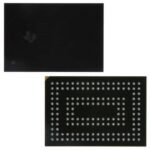 74SSTUB32865AZJBR

The activity of extra discounts on wholesale prices is in full swing…
Please fill in your contact information and we will send you the latest wholesale price list.





