 ChipApex | Global Electronic Components Supplier
SEARCH
Search Product
Search Post
— IC芯片 | 连接器 | 传感器 | 被动器件 —
Search productSearch post
— IC芯片 | 连接器 | 传感器 | 被动器件 —
Consult the customer manager about the wholesale price.
consultation hotline:86-132-6715-2157
email:[email protected]
Contact the product manager for consultation. One-stop consultation is available.
Do you want a lower wholesale price? Please send us your inquiry and we will reply immediately.
The 82V3202NLG is a dual Low Skew Clock Buffer manufactured by Renesas Electronics. It operates at a supply voltage of 3.3 V and provides four low skew outputs with full CMOS drive capability. The device features zero input-output delay, utilizing an on-chip Phase Locked Loop (PLL) for feedback obtained from the CLKOUT pad. Outputs can be generated directly from the input or via the PLL, supporting frequencies up to 133 MHz. It includes tri-state mode functionality for board-level testing and is packaged in an 8-pin SOIC format.
This component belongs to the family of high-speed clock buffers designed for low jitter and low skew applications. It utilizes advanced sub-micron CMOS process technology to achieve low phase noise performance. The device is available in industrial temperature ranges and supports both direct input buffering and PLL-based zero-delay buffering modes.
The device supports clock outputs from 10 to 133 MHz.
The PLL feedback is on-chip and is obtained from the CLKOUT pad.
Yes, the CLKIN input is 5 V tolerant.
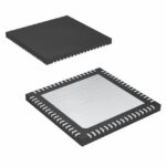 82V3202NLG
The activity of extra discounts on wholesale prices is in full swing…
Please fill in your contact information and we will send you the latest wholesale price list.






