 ChipApex | Global Electronic Components Supplier
SEARCH
Search Product
Search Post
— IC芯片 | 连接器 | 传感器 | 被动器件 —
Search productSearch post
— IC芯片 | 连接器 | 传感器 | 被动器件 —
Consult the customer manager about the wholesale price.
consultation hotline:86-132-6715-2157
email:[email protected]
Contact the product manager for consultation. One-stop consultation is available.
Do you want a lower wholesale price? Please send us your inquiry and we will reply immediately.
The 82V3391BEQG8 is a high-performance clock buffer manufactured by Renesas Electronics. It features one differential input and eight low-power HCSL (LP-HCSL) differential outputs, designed for distributing reference clocks in high-speed digital systems. The device operates on a single 3.3V supply voltage and supports input frequencies up to 500 MHz. It incorporates integrated output terminations compatible with both 100Ω and 85Ω transmission lines, reducing external component requirements. Packaged in a 4mm x 4mm 24-VFQFPN format, it offers low additive jitter and power consumption suitable for demanding datacom and telecom applications.
Verify the specific suffix 'QG8' against the manufacturer's current datasheet to confirm package type and tape-and-reel specifications. Ensure compatibility with the target PCB footprint for the 24-VFQFPN package. Check for any recent process change notices that may affect pinout or electrical characteristics prior to final procurement.
Select this component when a single reference clock must be distributed to multiple high-speed receivers requiring LP-HCSL signaling. Verify that the system requires integrated termination resistors to save board space. Confirm that the 3.3V operating voltage aligns with the rest of the system logic levels and that the 500 MHz maximum frequency meets the design requirements.
This part belongs to the 82V3391 family of clock buffers from Renesas. It serves as a fan-out buffer for generating multiple synchronized clock signals from a single source. The device is distinct from clock generators as it does not create new frequencies but rather replicates and conditions an existing input clock signal for distribution across a system.
Consult the official Renesas cross-reference guide for verified substitutes. Potential alternatives include other LP-HCSL clock buffers with similar I/O counts and termination options. Ensure any replacement maintains the same package dimensions and pinout if board space is constrained.
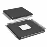 82V3391BEQG8
The activity of extra discounts on wholesale prices is in full swing…
Please fill in your contact information and we will send you the latest wholesale price list.







