 ChipApex | Global Electronic Components Supplier
SEARCH
Search Product
Search Post
— IC芯片 | 连接器 | 传感器 | 被动器件 —
Search productSearch post
— IC芯片 | 连接器 | 传感器 | 被动器件 —
Consult the customer manager about the wholesale price.
consultation hotline:86-132-6715-2157
email:[email protected]
Contact the product manager for consultation. One-stop consultation is available.
Do you want a lower wholesale price? Please send us your inquiry and we will reply immediately.
The 8308AGILF is a clock fanout buffer manufactured by Renesas Electronics, designed for high-speed signal distribution. It features eight LVCMOS or LVTTL outputs with a typical output impedance of 7Ω. The device accepts selectable LVCMOS_CLK or differential CLK and nCLK inputs. It operates within a supply voltage range of 3.135 V to 3.465 V and supports a maximum input frequency of 350 MHz. The component is housed in a 24-TSSOP package and functions reliably across an operating temperature range of -40°C to +85°C.
Verify the specific datasheet revision and RoHS compliance status directly with Renesas Electronics or authorized distributors before procurement. Confirm that the 24-TSSOP package dimensions and pin assignments match the target PCB layout requirements. Ensure the selected component meets the required operating temperature range and supply voltage specifications for the intended application environment.
Select this component when a single clock source needs to be distributed to multiple loads requiring LVCMOS or LVTTL logic levels. The 350 MHz maximum input frequency capability makes it suitable for demanding high-speed digital systems. Consider the 24-TSSOP surface-mount package for space-constrained designs requiring robust signal integrity through its low output impedance characteristics.
This part belongs to the Renesas clock buffer family, specifically engineered for fanout applications. It serves as a critical interface between clock generators and downstream logic components. The 8308AGILF variant provides eight outputs, distinguishing it from lower-output count models within the same series while maintaining compatible input interfaces and packaging standards.
Consult official Renesas documentation for verified cross-reference part numbers. Direct replacements must maintain identical pinout configurations, electrical parameters, and package dimensions to ensure compatibility without redesigning the host circuit board.
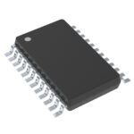 8308AGILF
The activity of extra discounts on wholesale prices is in full swing…
Please fill in your contact information and we will send you the latest wholesale price list.




