 ChipApex | Global Electronic Components Supplier

SEARCH
Search Product
Search Post
— IC芯片 | 连接器 | 传感器 | 被动器件 —
Search productSearch post
— IC芯片 | 连接器 | 传感器 | 被动器件 —
Consult the customer manager about the wholesale price.
consultation hotline:86-132-6715-2157
email:[email protected]
Contact the product manager for consultation. One-stop consultation is available.
Do you want a lower wholesale price? Please send us your inquiry and we will reply immediately.
The Renesas 83948AYI-147LF is a clock fan-out buffer and multiplexer IC designed for high-frequency signal distribution. It features a 2:12 input-to-output ratio with a maximum operating frequency of 350 MHz. The device supports multiple input logic standards including HCSL, LVCMOS, LVDS, LVHSTL, LVPECL, LVTTL, and SSTL, while providing LVCMOS and LVTTL outputs. Powered by a single supply voltage ranging from 2.375 V to 3.465 V, it operates within an industrial temperature range of -40°C to +85°C. The component is housed in a 32-LQFP surface-mount package.
This component is officially classified as obsolete and no longer manufactured by Renesas Electronics Corporation. Procurement is limited to existing stock or surplus channels. Verification of the specific manufacturing lot date code and authenticity is critical due to the end-of-life status. Designers should evaluate the available replacement options immediately to ensure long-term supply chain stability.
Select this part only if legacy design compatibility with specific Renesas clock architectures is required. Verify that the 350 MHz frequency limit meets system timing requirements. Ensure the PCB layout accommodates the 32-LQFP (7x7 mm) package dimensions. Consider the power supply noise immunity provided by the internal buffering when designing the power plane.
The 83948A series belongs to Renesas' portfolio of low-skew clock buffers and drivers. This specific variant integrates multiplexing capabilities to allow selection between different input sources. It is part of the broader family of timing solutions used in complex digital systems where signal integrity and phase alignment are paramount.
The onsemi NB3V8312CFAG is identified as a similar alternative part number. Engineers must verify pinout compatibility and electrical parameter equivalence before substitution.
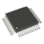 83948AYI-147LF

The activity of extra discounts on wholesale prices is in full swing…
Please fill in your contact information and we will send you the latest wholesale price list.





