 ChipApex | Global Electronic Components Supplier

SEARCH
Search Product
Search Post
— IC芯片 | 连接器 | 传感器 | 被动器件 —
Search productSearch post
— IC芯片 | 连接器 | 传感器 | 被动器件 —
Consult the customer manager about the wholesale price.
consultation hotline:86-132-6715-2157
email:[email protected]
Contact the product manager for consultation. One-stop consultation is available.
Do you want a lower wholesale price? Please send us your inquiry and we will reply immediately.
The Renesas 83948AYI-147LFT is a clock buffer and multiplexer IC featuring a 2:12 input-to-output ratio. It operates with a supply voltage range of 2.375V to 3.465V and supports a maximum frequency of 350 MHz. The device accepts multiple input formats including HCSL, LVCMOS, LVDS, LVHSTL, LVPECL, LVTTL, and SSTL, while providing LVCMOS or LVTTL outputs. Packaged in a 32-LQFP (7x7 mm) surface-mount case, it functions within an industrial temperature range of -40°C to 85°C. This component is classified as obsolete and no longer manufactured.
This part number is officially obsolete and has been discontinued by the manufacturer. Verification of current availability requires checking authorized distributors for remaining stock or end-of-life inventory. Replacement components should be evaluated based on pin compatibility and electrical specifications to ensure system continuity.
Designers requiring this specific 2:12 ratio and 350 MHz performance should verify if alternative clock buffers meet the required input/output voltage levels and package constraints. The transition from obsolete status necessitates reviewing pinout compatibility and thermal characteristics of potential substitute devices before integration.
The 83948A series belongs to Renesas' clock timing product line, specifically designed for fan-out buffering and signal conditioning. The 'I' suffix typically denotes the industrial temperature grade, while '147' indicates the specific speed bin and package variant within the family.
The onsemi NB3V8312CFAG is identified as a similar replacement option. Engineers must verify functional equivalence regarding input logic families, output drive strength, and pin assignment compatibility before substituting.
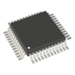 83948AYI-147LFT

The activity of extra discounts on wholesale prices is in full swing…
Please fill in your contact information and we will send you the latest wholesale price list.





