 ChipApex | Global Electronic Components Supplier

SEARCH
Search Product
Search Post
— IC芯片 | 连接器 | 传感器 | 被动器件 —
Search productSearch post
— IC芯片 | 连接器 | 传感器 | 被动器件 —
Consult the customer manager about the wholesale price.
consultation hotline:86-132-6715-2157
email:[email protected]
Contact the product manager for consultation. One-stop consultation is available.
Do you want a lower wholesale price? Please send us your inquiry and we will reply immediately.
The 8501BYLF is a clock buffer manufactured by Renesas Electronics Corporation, designed for high-speed signal distribution. It features a 1-to-16 fanout architecture with a single differential input and sixteen single-ended outputs. The device supports an input frequency of up to 500 MHz and operates on a 3.3V supply voltage. It is housed in a 48-pin TQFP package. The component accepts various input signaling standards including LVPECL, LVDS, HCSL, and HSTL, while providing HCSL-compatible outputs. It is suitable for applications requiring PCIe Gen1, Gen2, and Gen3 compliance.
Verify the specific datasheet revision and ordering information directly with authorized distributors or Renesas Electronics. Confirm that the 48-pin TQFP package matches your PCB footprint requirements. Ensure compatibility with 3.3V logic levels and check for any lead-free or RoHS compliance documentation required for your manufacturing process before finalizing procurement.
Select this component when a single differential clock source needs to drive up to sixteen loads with minimal skew. It is appropriate for designs requiring support for diverse input standards like LVDS or LVPECL while outputting HCSL signals. Consider the 500 MHz maximum frequency limit and the 3.3V operating voltage when evaluating system power and speed constraints against alternative buffer solutions.
This part belongs to Renesas' family of high-speed clock buffers and fanout drivers. These components are essential for maintaining signal integrity in complex digital systems where a master clock must be distributed to multiple synchronous devices. The 8501BYLF specifically addresses the need for high-frequency fanout in modern computing and communication architectures.
Consult official cross-reference lists for direct pin-compatible alternatives. Verify electrical specifications such as input/output voltage levels, maximum frequency, and package dimensions to ensure functional equivalence in existing designs.
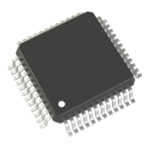 8501BYLF

The activity of extra discounts on wholesale prices is in full swing…
Please fill in your contact information and we will send you the latest wholesale price list.





