 ChipApex | Global Electronic Components Supplier

SEARCH
Search Product
Search Post
— IC芯片 | 连接器 | 传感器 | 被动器件 —
Search productSearch post
— IC芯片 | 连接器 | 传感器 | 被动器件 —
Consult the customer manager about the wholesale price.
consultation hotline:86-132-6715-2157
email:[email protected]
Contact the product manager for consultation. One-stop consultation is available.
Do you want a lower wholesale price? Please send us your inquiry and we will reply immediately.
The Renesas 85104AGILF is a high-performance clock fanout buffer and multiplexer designed for PCI Express applications. It features a 2:4 input-to-output ratio, supporting differential or LVCMOS/LVTTL inputs to four LVCMOS/LVTTL outputs. The device operates within a supply voltage range of 3.135V to 3.465V and functions across an industrial temperature range of -40°C to +85°C. Packaged in a 20-pin TSSOP, it integrates PLL functionality for precise clock generation and distribution.
Verify component authenticity through authorized channels due to potential counterfeit risks. Confirm package integrity and pin alignment against the official datasheet specifications. Ensure storage conditions comply with moisture sensitivity level requirements prior to soldering. Cross-reference ordering information with current manufacturer documentation to avoid obsolete variants.
Select this component when a design requires both signal buffering and source selection for critical clock lines. Evaluate input signal compatibility against available system references. Assess thermal performance within the target enclosure constraints. Consider footprint availability on the printed circuit board layout during initial schematic capture phases.
This part belongs to the 85104A family of clock management devices from Renesas Electronics. It serves as a specialized solution for managing complex clock topologies where signal integrity and timing precision are paramount. The device complements other series components by offering combined multiplexing and fanout functions in a compact surface-mount package.
Consult official substitution lists for direct replacements. Verify electrical parameter equivalence before implementation.
The datasheet specifies operation up to 700 MHz.
Yes, the device integrates a PLL for clock generation and jitter cleaning.
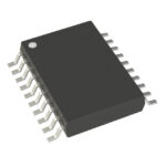 85104AGILF

The activity of extra discounts on wholesale prices is in full swing…
Please fill in your contact information and we will send you the latest wholesale price list.






