 ChipApex | Global Electronic Components Supplier

SEARCH
Search Product
Search Post
— IC芯片 | 连接器 | 传感器 | 被动器件 —
Search productSearch post
— IC芯片 | 连接器 | 传感器 | 被动器件 —
Consult the customer manager about the wholesale price.
consultation hotline:86-132-6715-2157
email:[email protected]
Contact the product manager for consultation. One-stop consultation is available.
Do you want a lower wholesale price? Please send us your inquiry and we will reply immediately.
The Renesas Electronics Corporation 8525BGLF is a clock buffer and multiplexer integrated circuit designed for high-speed signal distribution. It features a 1:4 input-to-output ratio, supporting a maximum operating frequency of 650 MHz. The device accepts differential CML or LVDS inputs and provides four differential LVPECL outputs. It operates within a supply voltage range of 3.135 V to 3.465 V and is housed in a 20-TSSOP package with a width of 4.40 mm. The component is rated for an industrial operating temperature range of 0°C to 70°C.
Verify the specific suffix 'GLF' against current manufacturer documentation to confirm RoHS compliance status and lead times, as availability may vary by region. Confirm that the 20-TSSOP package dimensions match the target PCB footprint requirements before finalizing procurement orders.
Select this component when a single differential source must drive four distinct LVPECL loads at frequencies up to 650 MHz. Ensure the system power supply can maintain the required 3.135 V to 3.465 V range. Verify that the input signal format matches either CML or LVDS standards to ensure proper logic level compatibility.
This part belongs to the ICS8525B family of clock buffers manufactured by Renesas Electronics. These devices are engineered for low jitter performance and are commonly used in digital signal processing applications requiring precise clock distribution. The GLF designation indicates a lead-free finish compliant with specific environmental directives.
Consult official Renesas cross-reference tools for verified pin-compatible alternatives. Generic substitutes may not match the specific 650 MHz frequency limit or LVPECL output characteristics.
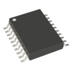 8525BGLF

The activity of extra discounts on wholesale prices is in full swing…
Please fill in your contact information and we will send you the latest wholesale price list.






