 ChipApex | Global Electronic Components Supplier

SEARCH
Search Product
Search Post
— IC芯片 | 连接器 | 传感器 | 被动器件 —
Search productSearch post
— IC芯片 | 连接器 | 传感器 | 被动器件 —
Consult the customer manager about the wholesale price.
consultation hotline:86-132-6715-2157
email:[email protected]
Contact the product manager for consultation. One-stop consultation is available.
Do you want a lower wholesale price? Please send us your inquiry and we will reply immediately.
The 854105AGLF is a low skew, high-performance 1-to-4 LVCMOS/LVTTL-to-LVDS clock fanout buffer manufactured by Renesas Electronics Corporation. It operates within an ambient temperature range of 0°C to 70°C and utilizes a 16-TSSOP package with a width of 4.40mm. The device supports an output frequency range up to 250MHz with an output skew of 55ps. It features one output bank delivering LVDS signals at 3.3V. The component is lead-free and RoHS compliant, currently classified as obsolete.
Verify the obsolete status before integration into new designs. Confirm availability through secondary market channels if existing inventory is required. Ensure the 16-TSSOP footprint matches the target PCB layout. Validate that the 3.3V LVDS output voltage aligns with downstream receiver specifications. Check for RoHS compliance documentation for regulatory adherence.
Choose this component when converting single-ended logic levels to differential LVDS is necessary. Consider the 250MHz maximum frequency limit for application suitability. Evaluate the 55ps skew specification against timing budget requirements. Assess the 1-to-4 fanout capability against load distribution needs. Verify thermal performance within the specified operating temperature range.
This part belongs to Renesas' family of clock buffer and driver integrated circuits designed for signal integrity optimization. It serves as a distribution element in complex digital architectures where noise immunity and timing precision are critical. The device bridges standard logic interfaces with high-speed differential transmission lines.
No public confirmed substitute part numbers are available for this obsolete component. Designers should evaluate newer Renesas LVDS buffer families or cross-reference compatible devices from other manufacturers based on pinout and electrical specifications.
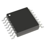 854105AGLF

The activity of extra discounts on wholesale prices is in full swing…
Please fill in your contact information and we will send you the latest wholesale price list.





