 ChipApex | Global Electronic Components Supplier

SEARCH
Search Product
Search Post
— IC芯片 | 连接器 | 传感器 | 被动器件 —
Search productSearch post
— IC芯片 | 连接器 | 传感器 | 被动器件 —
Consult the customer manager about the wholesale price.
consultation hotline:86-132-6715-2157
email:[email protected]
Contact the product manager for consultation. One-stop consultation is available.
Do you want a lower wholesale price? Please send us your inquiry and we will reply immediately.
The Renesas 8546AG-01LF is a low skew, 1-to-6 clock fanout buffer housed in a 24-TSSOP package. It provides six 3.3V or 2.5V LVDS outputs and accepts a selectable crystal oscillator or differential CLK1/nCLK1 pair as input. The device supports LVCMOS/LVTTL clock inputs and operates within a temperature range of 0°C to 70°C. It features a maximum frequency of 266 MHz and includes a multiplexer function for signal distribution.
Verify the specific ordering suffix (e.g., LF) to confirm lead-free status and package type. Ensure compatibility with system voltage requirements (3.3V or 2.5V). Confirm moisture sensitivity level and handling precautions during assembly. Cross-reference datasheet specifications against design constraints.
Select this component when low skew performance is critical for multi-output clock distribution. Consider the 24-TSSOP package size for board space constraints. Evaluate input flexibility requirements, specifically the need for crystal or differential input support. Verify thermal stability needs against the 0°C to 70°C operating range.
This part belongs to Renesas' family of clock buffers and timing ICs designed for high-speed data transmission applications. It serves as a fanout buffer to drive multiple loads from a single source while maintaining signal integrity. The device is suitable for systems requiring precise clock synchronization across multiple components.
Check for direct substitutes within the same product family that offer compatible pinouts and electrical characteristics. Verify if alternative packages are available for the same functional specification. Ensure any replacement maintains the required low skew and output drive capabilities.
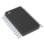 8546AG-01LF

The activity of extra discounts on wholesale prices is in full swing…
Please fill in your contact information and we will send you the latest wholesale price list.





