 ChipApex | Global Electronic Components Supplier

SEARCH
Search Product
Search Post
— IC芯片 | 连接器 | 传感器 | 被动器件 —
Search productSearch post
— IC芯片 | 连接器 | 传感器 | 被动器件 —
Consult the customer manager about the wholesale price.
consultation hotline:86-132-6715-2157
email:[email protected]
Contact the product manager for consultation. One-stop consultation is available.
Do you want a lower wholesale price? Please send us your inquiry and we will reply immediately.
The 854S054AGILF is a high-speed 4:1 differential-to-LVDS clock multiplexer manufactured by Renesas Electronics. It operates with four selectable differential clock inputs (PCLK, NPCLK) capable of accepting LVPECL, LVDS, or CML signal levels. The device translates any single-ended input signal to LVDS levels using resistor bias on the NPCLKX input. Key electrical parameters include a maximum output frequency of 2.5 GHz, a typical additive phase jitter of 0.147 ps RMS, and a maximum propagation delay of 700 ps. It functions within a supply voltage range of 3.135 V to 3.465 V and supports an ambient operating temperature from -40°C to +85°C.
The 854S054I belongs to the Renesas family of high-performance clock solutions. This specific variant is packaged in a 16-lead TSSOP format with dimensions of 5.0 x 4.4 x 1.0 mm and a 0.65 mm pitch. It is available in lead-free packages compliant with RoHS 6 standards.
The 854S058I is identified as a functional replacement offering 8:1 multiplexing capability. Designers should verify pinout compatibility and ensure the higher channel count does not impact board layout constraints.
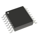 854S054AGILF

The activity of extra discounts on wholesale prices is in full swing…
Please fill in your contact information and we will send you the latest wholesale price list.




