 ChipApex | Global Electronic Components Supplier

SEARCH
Search Product
Search Post
— IC芯片 | 连接器 | 传感器 | 被动器件 —
Search productSearch post
— IC芯片 | 连接器 | 传感器 | 被动器件 —
Consult the customer manager about the wholesale price.
consultation hotline:86-132-6715-2157
email:[email protected]
Contact the product manager for consultation. One-stop consultation is available.
Do you want a lower wholesale price? Please send us your inquiry and we will reply immediately.
The ICS8743004DKILF is a FemtoClocks LVDS/LVPECL Zero Delay Buffer and Clock Generator designed for PCI Express and Ethernet applications. It features four differential output pairs with selectable pin types (LVDS or LVPECL) and supports independent frequency selection of 100MHz or 125MHz per pair. The device utilizes external feedback for zero-delay clock regeneration, ensuring low static and dynamic phase offset. Key electrical parameters include an output frequency range of 98MHz to 165MHz, an input frequency range of 19.6MHz to 165MHz, and a VCO range of 490MHz to 660MHz. It operates on a full 3.3V supply within an ambient temperature range of -40°C to 85°C.
Verify the component status as the source document indicates preliminary information. Confirm that the DKILF suffix corresponds to the lead-free RoHS 6 package variant in the 40-VFQFN format. Ensure compatibility with the specified 3.3V supply voltage and operating temperature range during sourcing.
Select this component when designing systems requiring precise clock regeneration with minimal phase offset for PCIe or Ethernet interfaces. Ensure the design maintains the VCO frequency between 490MHz and 660MHz by appropriately configuring the PDIV, FBI_DIV, and QDIV dividers. Verify that the required output count does not exceed the four available differential pairs.
This part belongs to the IDT/ICS FemtoClocks family of high-performance clock generators. It is specifically engineered to address jitter attenuation and frequency translation needs in high-speed serial communication standards like PCI Express and Ethernet, replacing older buffer solutions with lower phase noise characteristics.
Public confirmed substitute part numbers are not provided in the verified source material. Consult manufacturer documentation for cross-reference lists if alternative components are required.
The output type for the Q0/nQ0 through Q3/nQ3 pairs and FBOUT/nFBOUT is selected via the Q_TYPE pin. A logic low sets LVDS outputs (default), while a logic high sets LVPECL outputs.
These pins serve as a bidirectional M-LVDS interface. When OE_MLVDS is high, they act as outputs driven by the CLK/nCLK input divided by PDIV. When OE_MLVDS is low, they act as inputs for a reference clock from a backplane or other source.
Zero delay is achieved by using external feedback. The FBIN/nFBIN pins receive the regenerated clock signal from the FBOUT/nFBOUT pins, allowing the PLL to lock the output phase directly to the input reference phase.
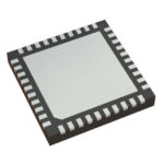 8743004DKILF

The activity of extra discounts on wholesale prices is in full swing…
Please fill in your contact information and we will send you the latest wholesale price list.






