 ChipApex | Global Electronic Components Supplier
SEARCH
Search Product
Search Post
— IC芯片 | 连接器 | 传感器 | 被动器件 —
Search productSearch post
— IC芯片 | 连接器 | 传感器 | 被动器件 —
Consult the customer manager about the wholesale price.
consultation hotline:86-132-6715-2157
email:[email protected]
Contact the product manager for consultation. One-stop consultation is available.
Do you want a lower wholesale price? Please send us your inquiry and we will reply immediately.
The 89H12NT12G2ZCHLGI is a PCIe Gen2 system interconnect switch manufactured by Renesas Electronics. It provides 12 lanes and 12 ports with non-blocking architecture for high-performance data transfer. The device supports a maximum clock frequency of 125 MHz and operates within a temperature range of -40°C to +85°C. Power requirements include voltages of 1 V, 2.5 V, and 3.3 V. It utilizes a 324-FCBGA package (19x19 mm) with surface mount installation. The component features a data rate of 96 Gb/s and supports 32/64-bit data bus widths.
Verify the obsolete status of this component before integration into new designs. Confirm moisture sensitivity level (MSL 3) handling requirements during storage and assembly. Ensure compatibility with existing PCB footprints for the 324-FCBGA package. Check for RoHS3 compliance documentation if required by regional regulations. Validate lead-free specifications against current manufacturing standards.
Select this model when 12 independent PCIe Gen2 ports are required without bandwidth contention. Consider the FCBGA package constraints for thermal management and board space. Evaluate the need for NTB functionality if isolated domain communication is necessary. Assess power supply complexity due to multiple voltage domains (1V, 2.5V, 3.3V). Compare against higher-lane alternatives if future scalability is anticipated.
This part belongs to the 89H12NT12G2 series of PCIe switches. It shares architectural similarities with other models in the family but offers a specific 12-lane configuration. The suffix ZCHLGI indicates specific packaging and environmental attributes defined by the manufacturer. It serves as a specialized interface IC for connecting multiple PCIe endpoints.
Publicly confirmed substitute part numbers include IDT89H12NT12G2ZCHLGI. Verify pin-to-pin compatibility and electrical parameters before substitution. Cross-reference datasheets for any minor revisions in the 89H12NT12G2 series.
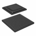 89H12NT12G2ZCHLGI
The activity of extra discounts on wholesale prices is in full swing…
Please fill in your contact information and we will send you the latest wholesale price list.






