 ChipApex | Global Electronic Components Supplier

SEARCH
Search Product
Search Post
— IC芯片 | 连接器 | 传感器 | 被动器件 —
Search productSearch post
— IC芯片 | 连接器 | 传感器 | 被动器件 —
Consult the customer manager about the wholesale price.
consultation hotline:86-132-6715-2157
email:[email protected]
Contact the product manager for consultation. One-stop consultation is available.
Do you want a lower wholesale price? Please send us your inquiry and we will reply immediately.
8P791208NLGI is listed in the Clock Buffers, Drivers range at ChipApex. The manufacturer field lists Renesas Electronics Corporation. Its product description is IC CLK DIV 2:8 700MHZ 32VFQFPN. Review the specifications below when checking this part for your BOM.
The 8P791208NLGI is a low additive jitter 2:8 clock buffer manufactured by Renesas Electronics. It accepts input frequencies from 1Hz to 700MHz and generates up to eight outputs. The device features two differential inputs supporting LVPECL, LVDS, LVHSTL, HCSL, or LVCMOS reference clocks. Outputs are arranged in two banks of four, each with independent power supplies. Output types include LVCMOS, LVDS, LVHSTL, and LVPECL. Key electrical parameters include a maximum output frequency of 700MHz, a maximum propagation delay of 2.25ns, and an operating supply voltage range of 1.71V to 3.465V. The component operates within a temperature range of -40°C to +85°C and is housed in a 32-VFQFN package.
Verify the specific ordering suffix NLGI against the manufacturer's current datasheet to confirm pinout, packaging dimensions, and moisture sensitivity level. Confirm RoHS compliance status and lead-free certification requirements prior to procurement. Ensure the selected variant matches the required output voltage levels and package type for the target PCB design.
Select this component when a 2:8 fanout ratio with low additive jitter is required for frequencies up to 700MHz. Verify that the system supports the available output voltage options (3.3V, 2.5V, 1.8V, 1.5V) and logic families. Ensure the design accommodates the 32-VFQFN package footprint and thermal requirements. Check if individual output enable functionality is necessary for the specific application topology.
The 8P791208NLGI belongs to the 8P791208 series of clock buffers. This series is designed for applications requiring flexible clock generation and distribution with minimal added jitter. The device integrates configurable output drivers and input selection logic into a compact QFN package, serving as a key component in complex timing architectures.
Consult the official Renesas replacement guide for verified cross-reference part numbers. Ensure any substitute component maintains compatibility with the required input/output voltage levels, package dimensions, and jitter specifications.
Explore related parts through Clock/Timing, Integrated Circuits (ICs), all product categories, ChipApex homepage.
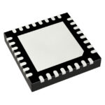 8P791208NLGI

The activity of extra discounts on wholesale prices is in full swing…
Please fill in your contact information and we will send you the latest wholesale price list.





