 ChipApex | Global Electronic Components Supplier

SEARCH
Search Product
Search Post
— IC芯片 | 连接器 | 传感器 | 被动器件 —
Search productSearch post
— IC芯片 | 连接器 | 传感器 | 被动器件 —
Consult the customer manager about the wholesale price.
consultation hotline:86-132-6715-2157
email:[email protected]
Contact the product manager for consultation. One-stop consultation is available.
Do you want a lower wholesale price? Please send us your inquiry and we will reply immediately.
8S89202BKILF is listed in the Clock Buffers, Drivers range at ChipApex. The manufacturer field lists Renesas Electronics Corporation. Its product description is IC CLK DIVIDER 1:8 3GHZ 32VFQFN. Review the specifications below when checking this part for your BOM.
The 8S89202 is a high-speed clock divider and distribution component manufactured by Renesas Electronics Corporation, originally designed by Integrated Device Technology. It functions as a low skew, 2:1 LVPECL multiplexer with a 1:8 fanout capability and internal termination. The device accepts differential inputs in LVPECL, LVDS, or CML formats and provides three banks of LVPECL outputs. Key electrical parameters include a maximum input frequency of 3 GHz and a maximum output frequency of 1.5 GHz. It operates on full 2.5V ±5% or 3.3V ±10% supply voltages within an ambient temperature range of -40°C to +85°C.
Verify the specific ordering suffix for packaging configuration. The 'BKILF' variant indicates a tray package, while 'BKILFT' denotes tape and reel with EIA-481-C pin orientation. The '/W' suffix specifies tape and reel with EIA-481-D pin orientation. Confirm RoHS compliance status and lead-free certification requirements against current manufacturing standards before procurement.
Select this component when designing systems requiring precise clock distribution with minimal skew across multiple loads. Ensure the input source matches the supported differential signaling levels (LVPECL, LVDS, CML). Verify that the PCB layout accommodates the 32-lead VFQFN package dimensions and includes thermal vias for the exposed pad to manage heat dissipation effectively under worst-case power conditions.
This device belongs to the IDT 8S89200 series of high-performance clock solutions. It was acquired by Renesas Electronics Corporation following the merger with IDT. The component serves as a specialized timing solution for high-speed digital interfaces, replacing older discrete buffer designs with integrated multiplexing and division capabilities in a compact form factor.
Publicly confirmed substitute part numbers are not available in the provided documentation. Designers should consult Renesas Electronics for current equivalent products or cross-reference with other manufacturers offering similar low-skew LVPECL dividers with internal termination if discontinuation occurs.
The IN and nIN pins feature built-in 50Ω resistors connected to the VT pin. This allows direct connection to LVDS, LVPECL, and CML drivers without external series or parallel termination resistors, simplifying the schematic and reducing component count.
These pins control the output division ratio for their respective output banks (A, B, and C). By setting these pins to logic high or low, users can independently configure each bank to operate at ÷1, ÷2, or ÷4 frequencies relative to the input clock.
Unused LVPECL output pairs can be left floating. However, it is recommended that no trace be attached to these pins to prevent potential noise coupling or signal integrity issues on the PCB.
Explore related parts through Clock/Timing, Integrated Circuits (ICs), all product categories, ChipApex homepage.
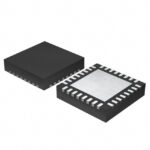 8S89202BKILF

The activity of extra discounts on wholesale prices is in full swing…
Please fill in your contact information and we will send you the latest wholesale price list.





