 ChipApex | Global Electronic Components Supplier

SEARCH
Search Product
Search Post
— IC芯片 | 连接器 | 传感器 | 被动器件 —
Search productSearch post
— IC芯片 | 连接器 | 传感器 | 被动器件 —
Consult the customer manager about the wholesale price.
consultation hotline:86-132-6715-2157
email:[email protected]
Contact the product manager for consultation. One-stop consultation is available.
Do you want a lower wholesale price? Please send us your inquiry and we will reply immediately.
8T3910BNLGI is listed in the Clock Buffers, Drivers range at ChipApex. The manufacturer field lists Renesas Electronics Corporation. Its product description is IC CLK BUF 3:11 500MHZ 48VFQFPN. Review the specifications below when checking this part for your BOM.
The IDT8T3910I is a high-performance clock fanout buffer manufactured by Integrated Device Technology, Inc. It accepts differential or crystal inputs and distributes the signal to ten differential outputs plus one single-ended reference output. The device supports LVPECL, LVDS, HCSL, and LVCMOS/LVTTL interface levels. Maximum operating frequencies are 500 MHz for differential outputs, 250 MHz for HCSL, and 200 MHz for LVCMOS. It operates on a 3.3V core supply with 3.3V or 2.5V output supplies, featuring low additive phase jitter of 0.22 ps typical.
Verify the manufacturer designation, as the component was originally produced by Integrated Device Technology, Inc., which has undergone corporate acquisitions. Confirm that the specific ordering suffix matches the required package and temperature range specifications from the official datasheet.
Select this component when a 3:11 ratio is required with mixed voltage domains. Ensure the output load termination matches the selected interface level (e.g., 50 ohms to VDDO-2V for LVPECL). Note that the LVCMOS output should be disabled if operating above 200 MHz.
This device belongs to the IDT8T3910 family of clock fanout buffers. It is functionally similar to the Renesas 8T39S10NLGI but differs in maximum frequency (500 MHz vs 2 GHz) and output configuration (ten differential outputs versus eleven).
Public confirmed substitute part numbers are not available in the provided documentation.
Explore related parts through Clock/Timing, Integrated Circuits (ICs), all product categories, ChipApex homepage.
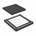 8T3910BNLGI

The activity of extra discounts on wholesale prices is in full swing…
Please fill in your contact information and we will send you the latest wholesale price list.





