 ChipApex | Global Electronic Components Supplier

SEARCH
Search Product
Search Post
— IC芯片 | 连接器 | 传感器 | 被动器件 —
Search productSearch post
— IC芯片 | 连接器 | 传感器 | 被动器件 —
Consult the customer manager about the wholesale price.
consultation hotline:86-132-6715-2157
email:[email protected]
Contact the product manager for consultation. One-stop consultation is available.
Do you want a lower wholesale price? Please send us your inquiry and we will reply immediately.
8T39S06ANBGI8 is listed in the Clock Buffers, Drivers range at ChipApex. The manufacturer field lists Renesas Electronics Corporation. Its product description is IC CLK BUFFER 3:7 2GHZ 36VFQFPN. Review the specifications below when checking this part for your BOM.
The Renesas 8T39S06ANBGI8 is a high-performance clock fanout buffer and multiplexer designed for signal distribution. It features three differential input pairs and seven differential output pairs, supporting maximum frequencies up to 2 GHz. The device accepts various input levels including HCSL, HSTL, LVDS, LVPECL, and crystal oscillators. It operates on dual supply voltages of 2.375V to 2.625V or 3.135V to 3.465V within an ambient temperature range of -40°C to +85°C. Packaged in a 36-VFQFPN (6x6 mm) surface-mount case with an exposed pad, it ensures low phase noise and precise clock distribution for high-speed digital systems.
Verify the specific ordering suffix ANBGI8 against official Renesas documentation to confirm package type and tape & reel configuration. Ensure compatibility with the required supply voltage range and input signal standards before integration. Cross-reference the 36-VFQFPN package dimensions with PCB layout guidelines to ensure proper thermal and electrical performance.
Select this component when a 3-to-7 fanout ratio is required with support for mixed input formats like crystal or differential signals. It is suitable for designs needing 2 GHz operation with strict jitter specifications. Compare against other series members if different output counts or pin configurations are needed. Confirm that the 36-pin VFQFPN package fits the available board space and thermal constraints.
This part belongs to the 8T39S family of clock buffers and multiplexers from Renesas Electronics. These devices are engineered for high-speed data transmission applications where signal integrity and low jitter are critical. The 8T39S06 variant specifically provides a 3-input to 7-output configuration, distinguishing it from other models with different ratios such as 1-to-8 or 2-to-10.
Check for direct substitutes within the 8T39S series with matching I/O ratios. Verify pin-to-pin compatibility if replacing existing components. Ensure that alternative parts support the same input/output voltage levels and frequency requirements.
Explore related parts through Clock/Timing, Integrated Circuits (ICs), all product categories, ChipApex homepage.
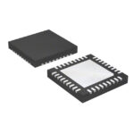 8T39S06ANBGI8

The activity of extra discounts on wholesale prices is in full swing…
Please fill in your contact information and we will send you the latest wholesale price list.






