 ChipApex | Global Electronic Components Supplier
8T49N222B-127NLGI8
Search Product
Search Post
— IC芯片 | 连接器 | 传感器 | 被动器件 —
Search productSearch post
— IC芯片 | 连接器 | 传感器 | 被动器件 —
Consult the customer manager about the wholesale price.
consultation hotline:86-132-6715-2157
email:[email protected]
Contact the product manager for consultation. One-stop consultation is available.
Do you want a lower wholesale price? Please send us your inquiry and we will reply immediately.
The 8T49N222B-127NLGI8 is a universal frequency translator IC belonging to the FemtoClock NG series by Renesas Electronics. It operates as a PLL-based device with bypass capability, supporting input formats including HCSL, LVDS, LVHSTL, LVPECL, and crystal sources. The component provides LVDS and LVPECL outputs and features a maximum operating frequency of 1.2 GHz. It utilizes a 48-VFQFN exposed pad package for surface mount installation. The device functions within a supply voltage range of 2.375V to 3.465V and supports an extended industrial temperature range from -40°C to 85°C.
Verify the specific suffix '127' against official Renesas documentation to confirm exact pinout and electrical characteristics, as variations exist within the FemtoClock NG family. Confirm RoHS compliance status through current manufacturer declarations. Ensure the 48-VFQFN package thermal pad requirements are met during PCB layout design to maintain reliable operation within the specified -40°C to 85°C temperature range.
Select this component when multi-standard input compatibility and high-frequency output generation are required. The integrated PLL with bypass offers flexibility for both jitter attenuation and direct pass-through applications. Consider the 48-VFQFN package size for space-constrained designs. Verify that the required output drive strength matches the LVDS or LVPECL loads in the target application circuit.
This part belongs to the FemtoClock NG series, designed for advanced clock management in complex digital systems. It serves as a universal frequency translator, bridging various input clock domains to standardized high-speed outputs. The series is characterized by low phase noise and high flexibility, making it suitable for next-generation networking and storage architectures where signal integrity is critical.
Consult the official Renesas FemtoClock NG product selector guide for direct replacements. Cross-reference alternative part numbers within the same series to ensure compatible package dimensions and electrical specifications. Verify that any substitute component maintains the required input/output format support and frequency capabilities for the specific application.
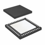 8T49N222B-127NLGI8
The activity of extra discounts on wholesale prices is in full swing…
Please fill in your contact information and we will send you the latest wholesale price list.






