 ChipApex | Global Electronic Components Supplier
8T49N240-034NLGI8
Search Product
Search Post
— IC芯片 | 连接器 | 传感器 | 被动器件 —
Search productSearch post
— IC芯片 | 连接器 | 传感器 | 被动器件 —
Consult the customer manager about the wholesale price.
consultation hotline:86-132-6715-2157
email:[email protected]
Contact the product manager for consultation. One-stop consultation is available.
Do you want a lower wholesale price? Please send us your inquiry and we will reply immediately.
The Renesas 8T49N240-034NLGI8 is a FemtoClock NG universal frequency translator and jitter attenuator. It operates with a supply voltage of 2.375V to 3.465V and supports input frequencies up to 875 MHz. The device provides four differential outputs capable of reaching 867 MHz, utilizing LVDS, LVPECL, or HCSL formats. Packaged in a 40-VFQFN (6mm x 6mm) with an exposed pad, it features dual inputs with signal loss monitoring. The component integrates OTP memory for configuration storage and includes three integer and one fractional output dividers.
Verify the specific suffix '034' against official Renesas documentation to confirm exact frequency programming and pinout compatibility. Confirm RoHS3 compliance status and check for End-of-Life notices via Product Change Notices. Ensure ESD handling protocols are followed during surface mount assembly of the VFQFN package.
Select this component when designing for 10G/40G/100G interfaces requiring low jitter margins. The 200 fs phase noise specification allows for cost-effective PCB designs compared to higher-jitter alternatives. Verify that the required output voltage levels match the available LVPECL, LVDS, or HCSL options provided by the device.
This part belongs to the Renesas FemtoClock NG family, designed for high-performance clock synthesis. It serves as a flexible solution for generating precise clock signals from various input sources, replacing multiple discrete clock generators and reducing board space requirements in high-speed digital systems.
Consult the official Renesas cross-reference guide for verified substitutes. Potential family members include other 8T49N240 variants with different suffixes or the 8T49N241 series for similar functionality.
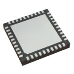 8T49N240-034NLGI8
The activity of extra discounts on wholesale prices is in full swing…
Please fill in your contact information and we will send you the latest wholesale price list.






