ChipApex | Global Electronic Components Supplier
8T49N240-991NLGI
Search Product
Search Post
— IC芯片 | 连接器 | 传感器 | 被动器件 —
Search productSearch post
— IC芯片 | 连接器 | 传感器 | 被动器件 —
Consult the customer manager about the wholesale price.
consultation hotline:86-132-6715-2157
email:[email protected]
Contact the product manager for consultation. One-stop consultation is available.
Do you want a lower wholesale price? Please send us your inquiry and we will reply immediately.
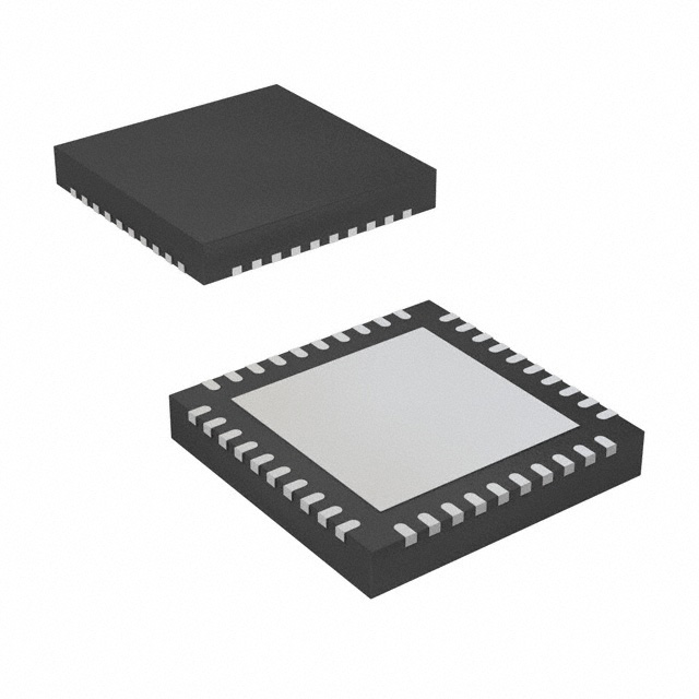
The 8T49N240-991NLGI is a FemtoClock NG Universal Frequency Translator manufactured by Renesas Electronics. It functions as a clock synthesizer and jitter attenuator, generating up to four differential output frequencies ranging from 8 kHz to 867 MHz. The device accepts various input levels including LVPECL, LVDS, and HCSL. Key electrical specifications include an operating supply voltage of 2.375 V to 3.465 V and a maximum operating temperature of +85 °C. It utilizes a 40-VFQFN package with exposed pad for surface mount installation.
Verify the specific suffix '991' against official Renesas documentation to confirm the exact factory pre-programmed frequency set and boot mode. Confirm availability status as distribution channels may report limited stock or end-of-life transitions following corporate acquisitions. Ensure compatibility with the required I2C address and EEPROM configuration file before ordering.
Select this component when designing for 10G/40G/100G Ethernet or SONET/SDH applications requiring low jitter performance under 200 fs. Compare against the 8T49N241 and 8T49N242 variants; note that the 8T49N240 lacks the fractional output divider found in the 8T49N241, limiting its frequency granularity compared to the newer models.
This part belongs to the FemtoClock NG family, which provides flexible timing solutions for high-speed serial interfaces. The 8T49N240 series is designed to replace discrete clock generators and fanout buffers, reducing PCB area and system cost. Note that Renesas timing products are transitioning to SiTime, affecting long-term support and procurement channels.
The 8T49N241-998NLGI and 8T49N242-998NLGI are direct functional upgrades within the same package footprint. The 8T49N241 adds a fractional output divider for finer frequency resolution, while the 8T49N242 supports higher output frequencies up to 1 GHz. Verify register compatibility if migrating between these variants.
 8T49N240-991NLGI
The activity of extra discounts on wholesale prices is in full swing…
Please fill in your contact information and we will send you the latest wholesale price list.