 ChipApex | Global Electronic Components Supplier

SEARCH
Search Product
Search Post
— IC芯片 | 连接器 | 传感器 | 被动器件 —
Search productSearch post
— IC芯片 | 连接器 | 传感器 | 被动器件 —
Consult the customer manager about the wholesale price.
consultation hotline:86-132-6715-2157
email:[email protected]
Contact the product manager for consultation. One-stop consultation is available.
Do you want a lower wholesale price? Please send us your inquiry and we will reply immediately.
8T49N242-999NLGI8 is listed in the Specialized ICS range at ChipApex. The manufacturer field lists Renesas Electronics Corporation. Its product description is IC FREQ TRANSLATOR 40VFQFPN. Review the specifications below when checking this part for your BOM.
The Renesas 8T49N242-999NLGI8 is a FemtoClock NG Universal Frequency Translator housed in a 40-VFQFPN (6x6mm) package. It features one fractional-feedback PLL and four integer output dividers, generating up to four independent output frequencies from 8kHz to 1GHz (differential) or 250MHz (LVCMOS). The device accepts two differential/single-ended input clocks (8kHz–875MHz) plus a fundamental-mode crystal (10MHz–50MHz). It supports LVPECL, LVDS, HCSL, and LVCMOS outputs with 2.5V/3.3V supply modes. Key specifications include 0.35ps RMS typical jitter (12kHz–20MHz), ±50ppb initial holdover accuracy, and I2C programmability.
Verify the ordering suffix '999' indicates factory pre-programmed configuration behavior distinct from other variants like '998'. Confirm RoHS 6 compliance and lead-free status. Ensure the 40-VFQFPN exposed pad thermal requirements are met during assembly. Check for specific PCNs regarding material or assembly site changes.
Select this component when four independent clock outputs are required with low jitter performance. Ensure input frequencies fall within the 8kHz to 875MHz range. Verify that the required output voltage levels (1.8V, 2.5V, or 3.3V) match the available VCCO supplies. Consider the need for hitless switching and holdover capabilities for synchronization applications.
The 8T49N242 belongs to the FemtoClock NG family of universal frequency translators. It integrates a fractional-feedback PLL with multiple integer output dividers. The device is designed for high-performance timing applications requiring flexible frequency synthesis and jitter attenuation across various communication standards.
Public confirmed substitute part numbers: 8T49N242-998NLGI8, 8T49N241-994NLGI8, 8T49N241-998NLGI8, 8T49N242-998NLGI, 8T49N242-999NLGI.
The maximum differential output frequency is 1.0 GHz.
The device monitors inputs for Loss of Signal (LOS) and supports automatic or manual hitless switching to a backup input. If no valid inputs remain, it enters holdover mode with ±50ppb initial accuracy.
Yes, the outputs can be configured as LVCMOS, providing up to eight single-ended outputs (using both Q and nQ pins) at frequencies up to 250 MHz.
Explore related parts through Integrated Circuits (ICs), all product categories, ChipApex homepage.
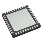 8T49N242-999NLGI8

The activity of extra discounts on wholesale prices is in full swing…
Please fill in your contact information and we will send you the latest wholesale price list.





