 ChipApex | Global Electronic Components Supplier
8T49N286-997NLGI
Search Product
Search Post
— IC芯片 | 连接器 | 传感器 | 被动器件 —
Search productSearch post
— IC芯片 | 连接器 | 传感器 | 被动器件 —
Consult the customer manager about the wholesale price.
consultation hotline:86-132-6715-2157
email:[email protected]
Contact the product manager for consultation. One-stop consultation is available.
Do you want a lower wholesale price? Please send us your inquiry and we will reply immediately.
The 8T49N286-997NLGI is a FemtoClock NG clock synthesizer and jitter cleaner manufactured by Renesas Electronics. It belongs to the 8T49N286A series, designed for high-performance timing applications requiring low phase noise. The device integrates multiple output buffers capable of generating precise clock signals from crystal or external reference inputs. Key specifications include RMS phase jitter performance typical of the FemtoClock NG architecture, supporting various differential output standards such as LVPECL and LVDS. It operates within an industrial temperature range and utilizes an I2C interface for register programming and configuration management.
Verify the specific suffix '997' against official Renesas documentation to confirm factory pre-programmed frequency configurations. Ensure compatibility with required output voltage levels and package type before integration. Confirm current availability status through authorized distributors as lead times may vary.
Select this component when low RMS phase jitter is critical for data integrity in high-speed interfaces. Compare jitter specs at relevant offset frequencies against system requirements. Verify that the available output drivers match the load capacitance and impedance of the receiving devices.
This part is part of the 8T49N286 family, which offers universal frequency translation capabilities. It serves as a replacement for older jitter attenuators in modern high-speed digital systems requiring precise clock distribution and noise filtering.
Check for direct pin-compatible upgrades within the 8T49N2xx series. Verify if newer revisions offer improved jitter performance or additional output options without requiring PCB redesign.
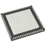 8T49N286-997NLGI
The activity of extra discounts on wholesale prices is in full swing…
Please fill in your contact information and we will send you the latest wholesale price list.






