 ChipApex | Global Electronic Components Supplier
8T49N286-998NLGI8
Search Product
Search Post
— IC芯片 | 连接器 | 传感器 | 被动器件 —
Search productSearch post
— IC芯片 | 连接器 | 传感器 | 被动器件 —
Consult the customer manager about the wholesale price.
consultation hotline:86-132-6715-2157
email:[email protected]
Contact the product manager for consultation. One-stop consultation is available.
Do you want a lower wholesale price? Please send us your inquiry and we will reply immediately.
The 8T49N286-998NLGI8 is a FemtoClock NG Universal Frequency Translator manufactured by Renesas Electronics. It operates within a supply voltage range of 2.375V to 3.465V and supports input levels including HCSL, LVCMOS, LVDSM, LVHSTL, LVPECL, and crystals. The device provides an input-to-output ratio of 5:8 with differential capabilities. It features a maximum frequency of 1GHz and is housed in a 72-VFQFN exposed pad package (10x10mm). The component functions as a clock synthesizer or jitter cleaner compliant with GR.1244 Stratum standards.
Verify the exact suffix against official documentation, as standard listings often use '998NLGI8'. Confirm moisture sensitivity level (MSL 3) and reflow soldering profiles prior to assembly. Ensure the specific order code matches the required factory pre-programmed configuration for the target application frequencies.
Select this model when a 5-input to 8-output frequency translation architecture is required. Verify that the 72-VFQFN package dimensions fit the PCB layout constraints. Ensure the design accommodates the 2.375V to 3.465V power supply requirements and I2C programming interface for register configuration.
This component belongs to the Renesas FemtoClock NG family, designed for low-jitter clock generation and distribution. It serves as a universal frequency translator capable of accepting various input references and generating multiple independent output frequencies up to 1GHz.
Direct pin-compatible replacements are not explicitly documented in public sources. Evaluate other models within the 8T49N286 series or the broader 8T49N2xx family for functional equivalence, ensuring input/output ratios and package types match.
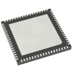 8T49N286-998NLGI8
The activity of extra discounts on wholesale prices is in full swing…
Please fill in your contact information and we will send you the latest wholesale price list.





