 ChipApex | Global Electronic Components Supplier
8T49N524NLG
Search Product
Search Post
— IC芯片 | 连接器 | 传感器 | 被动器件 —
Search productSearch post
— IC芯片 | 连接器 | 传感器 | 被动器件 —
Consult the customer manager about the wholesale price.
consultation hotline:86-132-6715-2157
email:[email protected]
Contact the product manager for consultation. One-stop consultation is available.
Do you want a lower wholesale price? Please send us your inquiry and we will reply immediately.
The IDT8T49N524I is a dual four-output programmable clock generator utilizing fourth-generation FemtoClock NG PLL technology. It features selectable LVPECL or LVDS outputs and supports input frequencies from 5MHz to 800MHz via crystal or reference clock. The device generates two independent output frequencies ranging from 15.234MHz to 645MHz, and 975MHz to 1290MHz. Typical RMS phase jitter is 0.282ps at 125MHz and 0.278ps at 156.25MHz (12kHz–20MHz). It operates on 2.5V or 3.3V supplies within a -40°C to 85°C temperature range.
Verify the specific ordering suffix to confirm programmed default frequencies, as these are factory-defined. Confirm voltage supply requirements (2.5V vs 3.3V) match the target application's power rails. Check package availability in the 40-lead VFQFN format. Ensure I2C address selection via ADDR_SEL pin aligns with system bus constraints.
Select this component when dual independent frequency outputs are required from a single reference source. Choose based on output swing requirements: LVPECL for higher speed/noise immunity or LVDS for lower power. Verify that the desired output frequencies fall within the supported ranges of 15.234MHz–645MHz or 975MHz–1290MHz. Use I2C programming for flexible configurations or FSEL pins for hardware-selectable defaults.
The IDT8T49N524I belongs to the FemtoClock NG family, designed for applications demanding superior phase noise performance. It integrates a VCO operating between 1950MHz and 2580MHz with fractional output dividers. The device allows bypassing the PLL for direct routing or enabling an input doubler. It is manufactured by Integrated Device Technology, now part of Renesas Electronics.
Direct replacements must support dual 4-output architectures with similar jitter specifications. Verify compatibility with existing I2C register maps if software reuse is intended. Consider packages such as the 40-lead VFQFN for footprint compatibility. Evaluate alternative models like the 8T49N028 or 8T49N242 if output count or frequency ranges differ significantly.
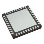 8T49N524NLG
The activity of extra discounts on wholesale prices is in full swing…
Please fill in your contact information and we will send you the latest wholesale price list.






