 ChipApex | Global Electronic Components Supplier
8V19N407Z-24NLGI
Search Product
Search Post
— IC芯片 | 连接器 | 传感器 | 被动器件 —
Search productSearch post
— IC芯片 | 连接器 | 传感器 | 被动器件 —
Consult the customer manager about the wholesale price.
consultation hotline:86-132-6715-2157
email:[email protected]
Contact the product manager for consultation. One-stop consultation is available.
Do you want a lower wholesale price? Please send us your inquiry and we will reply immediately.
The 8V19N407Z-24NLGI is a FemtoClock NG Jitter Attenuator and Clock Synthesizer designed for wireless infrastructure clock management. It features a two-stage PLL architecture where the first stage utilizes an external VCXO for jitter attenuation, and the second stage employs dual integrated VCOs (2400–2500MHz and 2920–3000MHz) for frequency synthesis. The device provides five differential configurable LVPECL/LVDS clock outputs and four differential LVDS SYSREF outputs. It supports JESD204B subclass 0 and 1 implementations with programmable phase alignment and delay capabilities.
Verify the specific suffix Z-24NLGI against the manufacturer's current production status, as availability may vary. Confirm that the required external VCXO component is sourced separately, as it is not included in the package. Ensure the design accommodates the 72-lead VFQFN thermal requirements for the -40°C to +85°C operating range.
Select this device when low phase noise performance is critical for high-speed data converters requiring JESD204B compliance. The dual VCO option allows selection between 2457.6MHz and 2949.12MHz center frequencies based on target output dividers. Ensure the system design includes provisions for an external VCXO and loop filter components to utilize the primary jitter attenuation feature.
This component belongs to the FemtoClock NG family from Renesas Electronics (formerly IDT). It is part of a series of high-performance clock synthesizers optimized for demanding timing applications in telecommunications and networking. The 8V19N408 variant serves as the functional basis for this model within the product line.
Direct replacements within the same family include other 8V19N40x variants, provided they support the required number of outputs and VCO configurations. Verify pin compatibility and register settings if substituting with other FemtoClock NG devices.
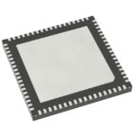 8V19N407Z-24NLGI
The activity of extra discounts on wholesale prices is in full swing…
Please fill in your contact information and we will send you the latest wholesale price list.





