 ChipApex | Global Electronic Components Supplier
8V19N474BFGI
Search Product
Search Post
— IC芯片 | 连接器 | 传感器 | 被动器件 —
Search productSearch post
— IC芯片 | 连接器 | 传感器 | 被动器件 —
Consult the customer manager about the wholesale price.
consultation hotline:86-132-6715-2157
email:[email protected]
Contact the product manager for consultation. One-stop consultation is available.
Do you want a lower wholesale price? Please send us your inquiry and we will reply immediately.
The 8V19N474BFGI is a FemtoClock NG Jitter Attenuator and Clock Synthesizer designed for high-performance clock conditioning. It features a two-stage PLL architecture utilizing an external VCXO for jitter attenuation and an internal 2500MHz VCO for frequency synthesis. The device provides five independent frequency dividers, including fractional-divider capabilities, to generate precise output frequencies. It supports LVDS and LVPECL output levels with a maximum input frequency of 2 GHz and operates on a single 3.3V supply.
Verify the specific suffix 'BFGI' against official Renesas documentation to confirm package type and moisture sensitivity level. Confirm current production status as FemtoClock products may have limited availability or obsolescence notices. Ensure the required external VCXO is compatible with the device's input specifications.
Select this component when low phase noise performance is critical for driving physical layer devices. The two-stage PLL design requires an external VCXO; ensure board space allows for this additional component. Verify that the required output frequencies can be synthesized using the available integer and fractional dividers from the target input range.
This part belongs to the 8V19N490A series within the FemtoClock family. It shares architectural similarities with other jitter attenuators in the lineup but is optimized for specific Ethernet and wireless applications requiring precise phase noise management and multiple clock outputs.
Direct replacements must support similar jitter attenuation specs and external VCXO requirements. Check for updated revisions within the 8V19N4xx series. Cross-model compatibility depends on pinout and register configuration alignment.
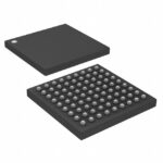 8V19N474BFGI
The activity of extra discounts on wholesale prices is in full swing…
Please fill in your contact information and we will send you the latest wholesale price list.







