 ChipApex | Global Electronic Components Supplier
8V49NS0412NLGI8
Search Product
Search Post
— IC芯片 | 连接器 | 传感器 | 被动器件 —
Search productSearch post
— IC芯片 | 连接器 | 传感器 | 被动器件 —
Consult the customer manager about the wholesale price.
consultation hotline:86-132-6715-2157
email:[email protected]
Contact the product manager for consultation. One-stop consultation is available.
Do you want a lower wholesale price? Please send us your inquiry and we will reply immediately.
The 8V49NS0412NLGI8 is a clock generator from the Renesas FemtoClock NS series, designed for high-performance timing applications. It features a wide VCO range of 1.92 GHz to 2.5 GHz and supports up to 12 output channels with selectable LVDS or LVPECL formats. The device integrates three fractional dividers and one integer divider, allowing flexible frequency synthesis. Key electrical parameters include a maximum output frequency of 2.5 GHz, an input frequency limit of 50 MHz, and a typical RMS phase jitter of 87 fs. It operates on a single 3.3 V supply within a -40°C to +85°C temperature range in a 64-pin VFQFN package.
Verify the specific suffix 'NLGI8' against official Renesas documentation to confirm packaging details, as distributor listings may vary between tray and reel configurations. Ensure compatibility with the required I2C address and boot source settings defined in the datasheet before finalizing procurement orders.
Select this component when multiple differential outputs are required with low jitter performance. Verify that the system design accommodates the 3.3 V supply voltage and the thermal requirements of the VFQFN-64 package. Confirm that the 50 MHz maximum input frequency meets the reference clock specifications of the target application.
This part belongs to the FemtoClock NS family, which provides advanced jitter attenuation and frequency translation capabilities. It serves as a successor to earlier FemtoClock generations, offering improved flexibility through fractional division and integrated boot memory for simplified system integration.
Direct replacements within the same series include the 8V49NS0312, which offers similar functionality but with different divider configurations. Cross-family alternatives such as the 8T49N287 series should be evaluated based on specific output count and jitter requirements.
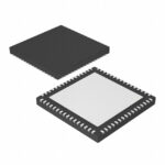 8V49NS0412NLGI8
The activity of extra discounts on wholesale prices is in full swing…
Please fill in your contact information and we will send you the latest wholesale price list.





