 ChipApex | Global Electronic Components Supplier

SEARCH
Search Product
Search Post
— IC芯片 | 连接器 | 传感器 | 被动器件 —
Search productSearch post
— IC芯片 | 连接器 | 传感器 | 被动器件 —
Consult the customer manager about the wholesale price.
consultation hotline:86-132-6715-2157
email:[email protected]
Contact the product manager for consultation. One-stop consultation is available.
Do you want a lower wholesale price? Please send us your inquiry and we will reply immediately.
8V54816ANLG is listed in the Application Specific Clock/Timing range at ChipApex. The manufacturer field lists Renesas Electronics Corporation. Its product description is NETWORK TIMING. Review the specifications below when checking this part for your BOM.
The 8V54816ANLG is a PCI Express (PCIe) clock and timing integrated circuit manufactured by Renesas Electronics Corporation. It operates with a maximum frequency of 350MHz and provides one output channel. The device utilizes LVDS input and output signaling standards. It is housed in a 100-VFQFPN package measuring 12x12 mm. The component supports a supply voltage range of 3.135V to 3.465V and functions within an operating temperature range of 0°C to 70°C.
Verify the current lifecycle status, as this component may be obsolete or discontinued. Confirm package compatibility and electrical specifications against the official datasheet before integration. Check for available replacement part numbers if new designs are required. Ensure compliance with relevant export control classifications such as EAR99.
Select this component for applications requiring precise PCIe clock generation and distribution. Consider the 350MHz frequency limit and LVDS signaling requirements. Evaluate the 100-VFQFPN package constraints for PCB layout. Verify that the 3.135V to 3.465V supply voltage aligns with system power rails.
This part belongs to Renesas' portfolio of clock and timing ICs designed for high-speed digital interfaces. It serves as a specialized solution for managing clock signals in complex electronic systems, particularly those adhering to PCI Express standards. The device integrates multiple functions into a single compact package to reduce board space.
Public confirmed substitute part numbers are not available in the provided documentation. Consult official manufacturer resources for potential obsolescence management strategies or equivalent alternatives.
Explore related parts through Clock/Timing, Integrated Circuits (ICs), all product categories, ChipApex homepage.
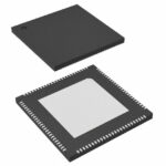 8V54816ANLG

The activity of extra discounts on wholesale prices is in full swing…
Please fill in your contact information and we will send you the latest wholesale price list.






