 ChipApex | Global Electronic Components Supplier

SEARCH
Search Product
Search Post
— IC芯片 | 连接器 | 传感器 | 被动器件 —
Search productSearch post
— IC芯片 | 连接器 | 传感器 | 被动器件 —
Consult the customer manager about the wholesale price.
consultation hotline:86-132-6715-2157
email:[email protected]
Contact the product manager for consultation. One-stop consultation is available.
Do you want a lower wholesale price? Please send us your inquiry and we will reply immediately.
8V79S674NLGI is listed in the Clock Buffers, Drivers range at ChipApex. The manufacturer field lists Renesas Electronics Corporation. Its product description is IC CLK BUF 1:4 2.5GHZ 20VFQFPN. Review the specifications below when checking this part for your BOM.
The 8V79S674NLGI is a clock divider and fanout buffer utilizing SiGe technology for high-frequency operation and low phase noise. It accepts differential LVCMOS or LVTTL inputs and provides four low-skew LVPECL outputs. The device supports frequency division ratios of ÷1, ÷2, ÷4, and ÷8, with a maximum output frequency of 2500 MHz in the ÷1 configuration. It operates on dual power supplies: 3.135V to 3.465V (nominal 3.3V) and 2.375V to 2.625V (nominal 2.5V). Packaged in a 20-lead VFQFN with an exposed pad, it functions within an ambient temperature range of -40°C to 85°C.
Verify component authenticity through authorized Renesas Electronics distributors. Confirm RoHS 6 compliance and lead-free status. Ensure proper handling of the 20-VFQFPN package due to moisture sensitivity. Validate thermal management requirements for the exposed pad during assembly.
Select this component when differential LVCMOS/LVTTL inputs must be converted to multiple LVPECL outputs. Ensure supply voltage matches either 3.3V or 2.5V domains. Verify that the required division ratio aligns with the N0/N1 pin logic. Consider thermal resistance characteristics for PCB layout design.
This part belongs to the 8V79S674 series of clock buffers and dividers. Originally manufactured by Integrated Device Technology (IDT), the product line was acquired by Renesas Electronics. The device serves as a specialized timing solution for high-speed digital systems requiring precise clock distribution.
The 8V79S674NLGI8 is functionally identical but supplied in tape and reel packaging instead of trays. No other cross-model substitutes are documented in the provided datasheet.
The division ratio is set using the N0 and N1 input pins: 0/0 for ÷1, 0/1 for ÷2, 1/0 for ÷4, and 1/1 for ÷8.
The maximum output skew between any two outputs under equal load conditions is 50 ps.
Yes, unused LVPECL outputs can be left floating without attached traces, though terminating both sides of the pair is also acceptable.
Explore related parts through Clock/Timing, Integrated Circuits (ICs), all product categories, ChipApex homepage.
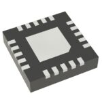 8V79S674NLGI

The activity of extra discounts on wholesale prices is in full swing…
Please fill in your contact information and we will send you the latest wholesale price list.






