 ChipApex | Global Electronic Components Supplier
8V89308ANLGI
Search Product
Search Post
— IC芯片 | 连接器 | 传感器 | 被动器件 —
Search productSearch post
— IC芯片 | 连接器 | 传感器 | 被动器件 —
Consult the customer manager about the wholesale price.
consultation hotline:86-132-6715-2157
email:[email protected]
Contact the product manager for consultation. One-stop consultation is available.
Do you want a lower wholesale price? Please send us your inquiry and we will reply immediately.
The 8V89308ANLGI is a Jitter Attenuator and FemtoClock Multiplier manufactured by Renesas Electronics Corporation. It operates on a single 3.3 V supply voltage, with an acceptable range of 3.135 V to 3.465 V. The device features a 1:2 input-to-output ratio and utilizes a 32-VFQFPN (5x5) package with an exposed pad for surface mount mounting. It supports LVPECL output type and functions within a temperature range of -40°C to +85°C. The typical operating supply current is 200 mA. This component is designed as a PLL-based synchronous multiplier.
Verify the exact part number suffix against official Renesas documentation to confirm specific package variants and tape-and-reel specifications. Ensure that the procurement channel provides valid traceability for automotive or industrial grade requirements if applicable. Confirm moisture sensitivity level handling procedures prior to assembly. Cross-reference the datasheet revision date to ensure compliance with current manufacturing standards and pinout configurations.
Select this component when utilizing Broadcom PHYs or Switches requiring precise clock synchronization and jitter reduction. Consider the LVPECL output requirement and 3.3 V supply constraints during system design. Evaluate the thermal performance within the specified -40°C to +85°C operating range. Verify that the 32-VFQFPN package footprint aligns with the PCB layout constraints and soldering capabilities.
This device belongs to the IDT 8V89308 series of clock generators and jitter attenuators. It is part of Renesas' portfolio following the acquisition of Integrated Device Technology. The series focuses on high-performance clock management for networking and telecommunications infrastructure, specifically targeting designs involving Broadcom semiconductor components for data path synchronization.
The IDT8V89308I is a closely related variant within the same product family. Verify functional equivalence and pin compatibility before substitution. Check for any differences in electrical characteristics or package options between the ANLGI suffix and other available variants in the 8V89308 series.
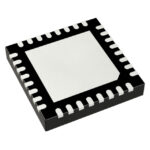 8V89308ANLGI
The activity of extra discounts on wholesale prices is in full swing…
Please fill in your contact information and we will send you the latest wholesale price list.






