 ChipApex | Global Electronic Components Supplier

SEARCH
Search Product
Search Post
— IC芯片 | 连接器 | 传感器 | 被动器件 —
Search productSearch post
— IC芯片 | 连接器 | 传感器 | 被动器件 —
Consult the customer manager about the wholesale price.
consultation hotline:86-132-6715-2157
email:[email protected]
Contact the product manager for consultation. One-stop consultation is available.
Do you want a lower wholesale price? Please send us your inquiry and we will reply immediately.
950811AGLFT is listed in the Application Specific Clock/Timing range at ChipApex. The manufacturer field lists Renesas Electronics Corporation. Its product description is IC FREQ GEN 200MHZ CLK 56-TSSOP. Review the specifications below when checking this part for your BOM.
The ICS950811 is a frequency generator designed for the Brookdale-Mobile chipset, providing clock signals for CPU and peripheral interfaces. It features three differential CPU clock pairs (66MHz to 200MHz), seven 33.3MHz PCI clocks, five 66.6MHz 3V66 clocks, and single outputs for USB, DOT, REF, and VCH at 48MHz or 66.6MHz. The device operates on a 3.3V supply with an operating temperature range of 0°C to +85°C. Key electrical specifications include CPU output jitter under 150ps, 3V66 output jitter under 250ps, and CPU output skew under 100ps. It supports spread spectrum modulation down to -0.5%.
Verify that the ordering suffix matches the required package type: 'G' indicates TSSOP, while 'F' indicates SSOP. Confirm the presence of 'LF' in the part number to ensure Lead-Free and RoHS compliance. Ensure the tape and reel designation 'T' is included if bulk packaging is required. Cross-reference the full part number against the manufacturer's current datasheet revision to confirm pinout and electrical characteristics have not changed.
Select this component when designing for the Brookdale-Mobile platform requiring integrated CPU, PCI, and 3V66 clock generation. Choose the TSSOP ('G') or SSOP ('F') package based on board space constraints and thermal requirements. Ensure the host controller supports the I2C interface for programming edge rates and enabling/disabling specific clock outputs via the register map.
Manufactured by Integrated Circuit Systems, Inc., which was later acquired by Renesas Electronics Corporation. This device belongs to the family of programmable clock generators used in Intel-based mobile architectures during the early 2000s. It serves as a central timing reference for the Northbridge and Southbridge components in laptop and mobile workstation designs.
Public confirmed substitute part numbers are not available in the provided documentation. When replacing, verify compatibility with the specific chipset generation (e.g., Brookdale) and ensure the replacement device supports the same I2C programming protocol and output voltage levels (3.3V).
When the PD# pin transitions low, PCI buffer clocks stop first, followed by the 66Buf clocks, then the CPU PLL clocks, and finally the 48MHz and REF clocks. The CPU outputs maintain a differential bias voltage during this state.
The maximum allowed current depends on the specific power group. For example, the VDDA (PLL1) and VDD48 groups have specific limits defined in the electrical characteristics, with typical operating currents around 229mA to 233mA under full load conditions.
No. Only CPU outputs configured in the I2C registers to be stoppable via CPU_STOP# will stop. The final state for stopped CPU signals is CPUT driven high and CPUC undriven.
Explore related parts through Clock/Timing, Integrated Circuits (ICs), all product categories, ChipApex homepage.
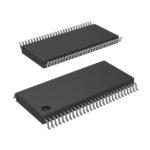 950811AGLFT

The activity of extra discounts on wholesale prices is in full swing…
Please fill in your contact information and we will send you the latest wholesale price list.






