 ChipApex | Global Electronic Components Supplier

SEARCH
Search Product
Search Post
— IC芯片 | 连接器 | 传感器 | 被动器件 —
Search productSearch post
— IC芯片 | 连接器 | 传感器 | 被动器件 —
Consult the customer manager about the wholesale price.
consultation hotline:86-132-6715-2157
email:[email protected]
Contact the product manager for consultation. One-stop consultation is available.
Do you want a lower wholesale price? Please send us your inquiry and we will reply immediately.
95V847AGLF is listed in the Application Specific Clock/Timing range at ChipApex. The manufacturer field lists Renesas Electronics Corporation. Its product description is IC CLK BUF DDR 233MHZ 1CIRC. Review the specifications below when checking this part for your BOM.
The Renesas 95V847AGLF is a zero-delay PLL clock buffer designed for DDR memory applications. It operates with a VDD and AVDD of 2.5V, supporting a maximum frequency of 233MHz. The device features one circuit with differential input and output, utilizing SSTL_2 levels. It is housed in a 24-TSSOP package (0.173" width) and functions within an operating temperature range of 0°C to 85°C.
This component is officially listed as obsolete by the manufacturer. Verification of end-of-life status is required before integration into new designs. Supply chain availability is limited to existing stock or secondary markets. Engineers should prioritize alternative components to ensure long-term production viability and supply chain stability.
Select this part only if legacy compatibility with 2.5V DDR architectures is mandatory. Verify that the 24-TSSOP footprint matches the PCB layout constraints. Confirm that the 233MHz maximum frequency meets the specific bus speed requirements of the target memory interface without necessitating higher-performance alternatives.
The 95V847A series belongs to Renesas' family of wide-range frequency clock drivers. These devices are engineered to provide stable clock signals for synchronous memory interfaces. The series typically includes variants with different pin counts and output configurations to support various DDR generations and system complexity levels.
Public confirmed substitute part numbers include CDCVF857DGG and CDCVF857DGGR from Texas Instruments.
Explore related parts through Clock/Timing, Integrated Circuits (ICs), all product categories, ChipApex homepage.
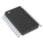 95V847AGLF

The activity of extra discounts on wholesale prices is in full swing…
Please fill in your contact information and we will send you the latest wholesale price list.






