 ChipApex | Global Electronic Components Supplier

SEARCH
Search Product
Search Post
— IC芯片 | 连接器 | 传感器 | 被动器件 —
Search productSearch post
— IC芯片 | 连接器 | 传感器 | 被动器件 —
Consult the customer manager about the wholesale price.
consultation hotline:86-132-6715-2157
email:[email protected]
Contact the product manager for consultation. One-stop consultation is available.
Do you want a lower wholesale price? Please send us your inquiry and we will reply immediately.
9DB102BGILF is listed in the Application Specific Clock/Timing range at ChipApex. The manufacturer field lists Renesas Electronics Corporation. Its product description is IC CLK FANOUT/BUFF ZD 20TSSOP. Review the specifications below when checking this part for your BOM.
The Renesas 9DB102BGILF is a zero-delay buffer and jitter attenuator designed for PCI Express (PCIe) applications. It features a single PLL circuit with one differential input and two differential outputs, operating at frequencies up to 101 MHz. The device utilizes HCSL output logic and requires a supply voltage between 3.135 V and 3.465 V. Manufactured by Renesas Electronics Corporation, it is housed in a 20-pin TSSOP package with a width of 4.40 mm. The component supports an industrial temperature range from -40°C to +85°C.
Verify the specific suffix 'I' against official documentation to confirm the extended industrial temperature rating (-40°C to +85°C). Confirm RoHS compliance status and check for active manufacturing or obsolescence notices directly from Renesas Electronics before procurement planning.
Select this component when a 1:2 differential clock split with jitter attenuation is required for PCIe Gen1/Gen2 interfaces. Ensure the design accommodates the 20-TSSOP footprint and that the system power rail aligns with the specified 3.135 V to 3.465 V operating window.
This part belongs to the 9DB102 family of zero-delay buffers. Variants such as 9DB102BFLFT and 9DB102BGLFT share similar electrical characteristics but differ in package types (SSOP vs. TSSOP) and commercial temperature ranges. The 'I' suffix typically denotes industrial grade specifications.
Direct substitutes include other members of the 9DB102 series, such as 9DB102BGLFT, provided the package and temperature requirements match. Verify pin compatibility and electrical parameters against the datasheet before substitution.
Explore related parts through Clock/Timing, Integrated Circuits (ICs), all product categories, ChipApex homepage.
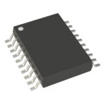 9DB102BGILF

The activity of extra discounts on wholesale prices is in full swing…
Please fill in your contact information and we will send you the latest wholesale price list.





