 ChipApex | Global Electronic Components Supplier

SEARCH
Search Product
Search Post
— IC芯片 | 连接器 | 传感器 | 被动器件 —
Search productSearch post
— IC芯片 | 连接器 | 传感器 | 被动器件 —
Consult the customer manager about the wholesale price.
consultation hotline:86-132-6715-2157
email:[email protected]
Contact the product manager for consultation. One-stop consultation is available.
Do you want a lower wholesale price? Please send us your inquiry and we will reply immediately.
9DB104BFLF is listed in the Application Specific Clock/Timing range at ChipApex. The manufacturer field lists Renesas Electronics Corporation. Its product description is IC BUFFER 4OUTPUT DIFF 28SSOP. Review the specifications below when checking this part for your BOM.
The Renesas Electronics 9DB104BFLF is a four-output differential clock buffer designed for PCI-Express applications. It operates within a supply voltage range of 3.135 V to 3.465 V and supports maximum input frequencies up to 220 MHz. The device provides four 0.7V current-mode differential output pairs with cycle-cycle jitter under 50 ps and output skew under 50 ps. It features an integrated PLL supporting zero-delay buffer mode, SMBus configuration capabilities, and spread spectrum modulation tolerance. The component is housed in a 28-pin SSOP package.
The 9DB104BFLF is marked as not recommended for new designs and has reached end-of-life status. Verification of availability requires checking specific distributor channels for remaining stock or obsolete inventory. Designers should consider the EOL status when planning long-term production runs.
Select this component only if legacy compatibility with Intel DB400 specifications is required. Ensure the design accommodates the 28-pin SSOP footprint and the external 475 ohm reference resistor on the IREF pin. Verify that the 3.3V nominal supply voltage aligns with the system power rails.
Originally manufactured by Integrated Circuit Systems, Inc. (ICS), this part was acquired by Renesas Electronics. It belongs to the 9DB series of differential buffers. The 'LF' suffix indicates lead-free and RoHS compliance. The device follows the Intel DB400 specification for differential buffering.
Public confirmed substitute: 9ZXL0451EKILFT (Renesas Electronics Corporation).
The output current is established by the IREF pin, which requires a fixed precision resistor tied to ground. A standard value of 475 ohms is typically used.
This pin selects the operating mode. A logic low selects Bypass (fan-out) mode, while a logic high selects PLL (zero-delay buffer) mode.
Yes, it is tolerant to triangular modulation down spread of 0 to -0.5% and center spread of +/- 0.25%.
Explore related parts through Clock/Timing, Integrated Circuits (ICs), all product categories, ChipApex homepage.
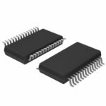 9DB104BFLF

The activity of extra discounts on wholesale prices is in full swing…
Please fill in your contact information and we will send you the latest wholesale price list.






