 ChipApex | Global Electronic Components Supplier
9DB202CFLFT
Search Product
Search Post
— IC芯片 | 连接器 | 传感器 | 被动器件 —
Search productSearch post
— IC芯片 | 连接器 | 传感器 | 被动器件 —
Consult the customer manager about the wholesale price.
consultation hotline:86-132-6715-2157
email:[email protected]
Contact the product manager for consultation. One-stop consultation is available.
Do you want a lower wholesale price? Please send us your inquiry and we will reply immediately.
The 9DB202CFLFT is a PCI Express jitter attenuator and multiplexer manufactured by Renesas Electronics Corporation. It operates with a maximum frequency of 140MHz and features one output channel. The device utilizes a Phase-Locked Loop (PLL) for clock signal processing and supports differential input and output signaling. It is designed to function within a supply voltage range of 3.135V to 3.465V and operates at temperatures between 0°C and 70°C. The component is housed in a 20-TSSOP package with a width of 4.40mm, intended for surface-mount installation.
Verify the specific suffix 'CFLFT' against official Renesas documentation to confirm RoHS compliance and lead-free status, as datasheets may list variations such as 'CGLF'. Confirm current production status, as related models in this series have been marked as obsolete or discontinued in public distributor records. Ensure the ordering part number matches the exact package and temperature grade required for the design.
Select this component when a single-output jitter attenuator with PLL functionality is required for PCI Express signals up to 140MHz. Verify that the system power supply remains within the 3.135V to 3.465V range. Check compatibility with available input clock formats (HCSL, LVDS, etc.) and ensure the 20-TSSOP footprint fits the PCB layout constraints. Consider thermal performance within the 0°C to 70°C operating range.
This part belongs to the 9DB202 family of PCI Express jitter attenuators from Renesas. Variants in this family, such as the 9DB202CGLF, share similar core specifications but may differ in packaging, temperature ratings, or environmental compliance suffixes. The 9DB202 series is distinct from buffer-only devices like the 9DB102 or zero-delay buffers like the 9DBU series.
Publicly available substitute part numbers are not confirmed for the 9DB202CFLFT. Related variants within the same family, such as 9DB202CGLF, may offer functional equivalence but require verification of package and environmental specifications. No cross-model substitutes are listed in the provided data.
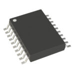 9DB202CFLFT
The activity of extra discounts on wholesale prices is in full swing…
Please fill in your contact information and we will send you the latest wholesale price list.





