 ChipApex | Global Electronic Components Supplier
9DB202CGLF
Search Product
Search Post
— IC芯片 | 连接器 | 传感器 | 被动器件 —
Search productSearch post
— IC芯片 | 连接器 | 传感器 | 被动器件 —
Consult the customer manager about the wholesale price.
consultation hotline:86-132-6715-2157
email:[email protected]
Contact the product manager for consultation. One-stop consultation is available.
Do you want a lower wholesale price? Please send us your inquiry and we will reply immediately.
The Renesas 9DB202CGLF is a PCI Express jitter attenuator and multiplexer IC designed for PCIe applications. It features a single PLL circuit with a 1:2 input-to-output ratio, supporting differential inputs and outputs. The device operates within a supply voltage range of 3.135V to 3.465V and supports a maximum frequency of 140MHz. It accepts HCSL, LVDS, LVHSTL, LVPECL, and SSTL input signals, providing HCSL outputs. Packaged in a 20-TSSOP (4.40mm wide) surface-mount housing, it functions within an operating temperature range of 0°C to 70°C.
Verify component status as the 9DB202CGLF is listed as obsolete by the manufacturer. Confirm availability through authorized distributors or secondary market suppliers. Ensure RoHS compliance documentation matches specific production batches. Check for alternative lead times due to end-of-life status. Validate package integrity upon receipt.
Select this component when designing PCIe Gen 1-3 systems requiring jitter attenuation and input multiplexing. Ensure the design accommodates the 20-TSSOP package dimensions and 0°C to 70°C industrial temperature range. Verify that input signal levels match supported formats (HCSL, LVDS, etc.). Consider power supply constraints within the 3.135V to 3.465V range during PCB layout.
The 9DB202CGLF belongs to the Renesas 9DB202 family of PCIe clock generators and jitter attenuators. It serves as a specialized timing solution for maintaining signal integrity in high-speed serial interfaces. The 'GLF' suffix typically denotes the tape-and-reel packaging variant and RoHS-compliant material composition within the broader product line.
RC19013A100GNG#KB0 is identified as a manufacturer-recommended replacement for the 9DB1200 series; however, direct substitution for the 9DB202CGLF requires verification of pin compatibility and functional equivalence against current inventory options.
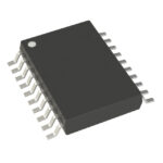 9DB202CGLF
The activity of extra discounts on wholesale prices is in full swing…
Please fill in your contact information and we will send you the latest wholesale price list.






