 ChipApex | Global Electronic Components Supplier
9DB202CGLFT
Search Product
Search Post
— IC芯片 | 连接器 | 传感器 | 被动器件 —
Search productSearch post
— IC芯片 | 连接器 | 传感器 | 被动器件 —
Consult the customer manager about the wholesale price.
consultation hotline:86-132-6715-2157
email:[email protected]
Contact the product manager for consultation. One-stop consultation is available.
Do you want a lower wholesale price? Please send us your inquiry and we will reply immediately.
The Renesas 9DB202CGLFT is a PCI Express jitter attenuator and multiplexer IC designed for high-speed serial link applications. It features an integrated Phase-Locked Loop (PLL) to reduce input clock jitter while maintaining signal integrity. The device accepts differential inputs including LVDS, LVPECL, HCSL, LVHSTL, and SSTL, converting them to a single differential HCSL output. Operating at a maximum frequency of 140MHz with a supply voltage range of 3.135V to 3.465V, it is housed in a 20-TSSOP package. This component supports PCIe Common Clocked architectures by providing precise clock distribution.
Verify the specific suffix 'GLFT' against the manufacturer's current datasheet to confirm pinout compatibility and RoHS status. Note that this component may be subject to End-of-Life (EOL) notices; check official Renesas Product Change Notifications (PCN) for availability and lifecycle status before finalizing procurement plans.
Select this component when a low-jitter, single-output HCSL clock is required from various differential input sources for PCIe Gen 1 or Gen 2 interfaces. Ensure the input clock frequency does not exceed 140MHz. Verify that the system power supply remains within the 3.135V to 3.465V range to maintain timing specifications.
The 9DB202CGLFT belongs to the Renesas 9DB202 family of PCIe jitter attenuators. It serves as a specialized clock conditioning solution distinct from standard clock buffers or generators. The part is engineered specifically to meet the stringent jitter requirements of PCI Express standards, differentiating it from general-purpose timing ICs.
Publicly confirmed substitute part numbers are not available in the provided documentation. Consult Renesas technical support for direct replacements or verify if newer revisions of the 9DB202 series offer equivalent functionality.
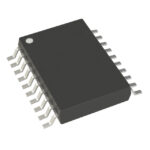 9DB202CGLFT
The activity of extra discounts on wholesale prices is in full swing…
Please fill in your contact information and we will send you the latest wholesale price list.





