 ChipApex | Global Electronic Components Supplier
9DB233AGILFT
Search Product
Search Post
— IC芯片 | 连接器 | 传感器 | 被动器件 —
Search productSearch post
— IC芯片 | 连接器 | 传感器 | 被动器件 —
Consult the customer manager about the wholesale price.
consultation hotline:86-132-6715-2157
email:[email protected]
Contact the product manager for consultation. One-stop consultation is available.
Do you want a lower wholesale price? Please send us your inquiry and we will reply immediately.
The Renesas Electronics 9DB233AGILFT is a PCI Express (PCIe) fanout buffer and zero-delay clock distribution IC. It features one differential input and two differential outputs, operating at frequencies up to 110 MHz. The device utilizes HCSL output signaling and supports a supply voltage range of 3.135 V to 3.465 V. Packaged in a 20-TSSOP format with a pitch of 4.40 mm, it is designed for low jitter applications compliant with PCIe Gen1 through Gen3 standards.
Verify the specific suffix 'ILFT' against the manufacturer's current datasheet to confirm package dimensions and temperature grade. Ensure compatibility with the target PCB footprint for the 20-TSSOP package. Confirm RoHS compliance status as per the latest environmental declarations before finalizing procurement orders.
Select this component when a single differential source requires splitting into two matched differential loads with minimal skew. Verify that the system power supply remains within the 3.135 V to 3.465 V range. Consider the 20-TSSOP package constraints if board space is limited compared to larger packages like QFN or BGA.
This part belongs to the 9DB233 series of PCIe clock buffers. It serves as a critical timing element in systems where clock integrity is paramount. The 'A' typically denotes an advanced revision or specific binning, while 'ILFT' indicates the industrial temperature range and tape-and-reel packaging format.
Direct pin-to-pin replacements may include other Renesas 9DB233 variants with different suffixes indicating package or temperature changes. Cross-vendor equivalents require careful verification of HCSL swing levels and PLL bandwidth characteristics to ensure signal integrity is maintained.
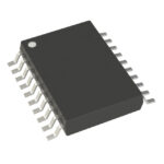 9DB233AGILFT
The activity of extra discounts on wholesale prices is in full swing…
Please fill in your contact information and we will send you the latest wholesale price list.





