 ChipApex | Global Electronic Components Supplier
9DB403DFLFT
Search Product
Search Post
— IC芯片 | 连接器 | 传感器 | 被动器件 —
Search productSearch post
— IC芯片 | 连接器 | 传感器 | 被动器件 —
Consult the customer manager about the wholesale price.
consultation hotline:86-132-6715-2157
email:[email protected]
Contact the product manager for consultation. One-stop consultation is available.
Do you want a lower wholesale price? Please send us your inquiry and we will reply immediately.
The Renesas Electronics 9DB403DFLFT is a clock buffer IC designed for PCI Express applications, supporting Gen1 and Gen2 standards. It features four outputs with HCSL output types and accepts clock inputs up to 400 MHz. The device operates within a supply voltage range of 3.135 V to 3.465 V and consumes 125 mA of operating current. Packaged in a 28-SSOP format, it functions between 0°C and +70°C. Key electrical parameters include a maximum propagation delay of 0 ps and a maximum duty cycle of 55%.
Verify the specific suffix 'FLFT' against the manufacturer's datasheet to confirm package type and tape-and-reel specifications. Confirm RoHS compliance status directly from the official documentation, as regulatory details may vary by production batch or region. Ensure the ordering quantity matches the standard factory pack size of 1500 units if full reels are required.
Select this component when a single-clock source must drive four distinct loads with minimal skew in PCIe architectures. Verify that the system power supply can maintain the 3.135 V to 3.465 V range under load. Check that the SSOP-28 footprint aligns with the PCB layout constraints and thermal requirements for the 125 mA operating current.
This part belongs to the 9DB403 series of clock buffers. It is functionally related to other members like the 9DB803DFLFT, which provides eight outputs in an SSOP-48 package. The 'ICS' prefix alias indicates its heritage within the Integrated Circuit Systems product line now managed by Renesas.
The 9DB803DFLFT serves as a higher-channel alternative with eight outputs in an SSOP-48 package. Direct pin-to-pin substitution is not possible due to the different package sizes and pin counts. Evaluate system design changes if upgrading to the 8-output variant.
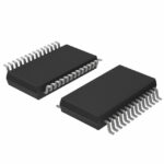 9DB403DFLFT
The activity of extra discounts on wholesale prices is in full swing…
Please fill in your contact information and we will send you the latest wholesale price list.





