 ChipApex | Global Electronic Components Supplier
9DB433AFILF
Search Product
Search Post
— IC芯片 | 连接器 | 传感器 | 被动器件 —
Search productSearch post
— IC芯片 | 连接器 | 传感器 | 被动器件 —
Consult the customer manager about the wholesale price.
consultation hotline:86-132-6715-2157
email:[email protected]
Contact the product manager for consultation. One-stop consultation is available.
Do you want a lower wholesale price? Please send us your inquiry and we will reply immediately.
The Renesas Electronics 9DB433AFILF is a four-output PCIe Gen1-Gen3 zero-delay buffer (ZDB) and fanout clock distribution IC. It operates on a single 3.3V supply with a voltage range of 3.135V to 3.465V. The device accepts differential HCSL inputs and provides four pairs of differential HCSL outputs, supporting maximum frequencies up to 166 MHz. Packaged in a 28-pin SSOP, it features phase jitter performance compliant with PCIe Gen3 standards (<1ps rms). The component supports both zero-delay buffer mode and fanout mode, accommodating spread spectrum input signals for low EMI applications.
Verify the specific package variant against design requirements, as the base model 9DB433 is available in both SSOP and TSSOP packages. Confirm that the SSOP-28 footprint matches the PCB layout constraints. Ensure the operating temperature range aligns with the target industrial or commercial environment specifications before finalizing procurement.
Select this component when a four-channel differential clock buffer with zero-delay feedback is required for PCIe interfaces. The 9DB433AFILF is suitable for designs needing backward compatibility across PCIe generations while maintaining strict jitter budgets. Verify that the input source can provide the necessary differential HCSL signal levels for proper operation within the specified 3.3V power domain.
This part belongs to the 9DB433 family of high-performance clock buffers designed specifically for PCI Express applications. It serves as a critical timing element in systems requiring precise synchronization between the clock generator and multiple peripheral devices. The device integrates PLL functionality to support bandwidth programming from 33MHz to 110MHz in PLL mode.
The 9DB433AGLF is a pin-compatible alternative featuring a TSSOP-28 package instead of SSOP-28. Both parts share identical electrical characteristics and functionality, differing only in the physical housing dimensions and lead configuration.
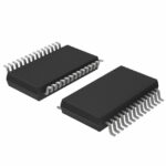 9DB433AFILF
The activity of extra discounts on wholesale prices is in full swing…
Please fill in your contact information and we will send you the latest wholesale price list.







