 ChipApex | Global Electronic Components Supplier
9DB433AGLF
Search Product
Search Post
— IC芯片 | 连接器 | 传感器 | 被动器件 —
Search productSearch post
— IC芯片 | 连接器 | 传感器 | 被动器件 —
Consult the customer manager about the wholesale price.
consultation hotline:86-132-6715-2157
email:[email protected]
Contact the product manager for consultation. One-stop consultation is available.
Do you want a lower wholesale price? Please send us your inquiry and we will reply immediately.
The Renesas Electronics 9DB433AGLF is a four-output PCIe Gen1/Gen2/Gen3 zero-delay buffer (ZDB) and fanout clock buffer. It operates within a supply voltage range of 3.135 V to 3.465 V, supporting maximum input frequencies up to 166 MHz and maximum output frequencies up to 100 MHz. The device features a propagation delay of 0 ps and maintains a duty cycle of no more than 55%. Designed for surface-mount installation, it is housed in a TSSOP-28 package with an operating temperature range from 0°C to +70°C.
Verify the specific suffix 'AGLF' against official Renesas documentation to confirm RoHS compliance and lead-free status. Confirm that the TSSOP-28 package variant matches the design requirements, as other suffixes may indicate different packaging or temperature ranges. Ensure the source document explicitly lists this part number as active or available for procurement.
Select the 9DB433AGLF when a four-channel clock buffer is required for PCIe applications with strict jitter specifications. This component is suitable for designs needing zero-delay buffering capabilities to minimize skew between the reference and output clocks. Verify that the input signal originates from a compatible differential source pair and that the power supply constraints fit within the 3.135V to 3.465V window.
The 9DB433AGLF belongs to the 9DB433 series of clock buffers manufactured by Renesas Electronics. It is functionally related to other models in the family, such as the 9DB833 which provides eight outputs, and the 9DB233 which offers two outputs. These components share similar PCIe compatibility features but differ in output count and package configurations.
Publicly confirmed substitute part numbers are not provided in the available data. Designers should consult the official Renesas replacement guide or contact the manufacturer directly for qualified alternatives if this specific part number becomes unavailable.
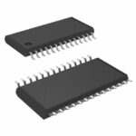 9DB433AGLF
The activity of extra discounts on wholesale prices is in full swing…
Please fill in your contact information and we will send you the latest wholesale price list.






