 ChipApex | Global Electronic Components Supplier
9DB433AGLFT
Search Product
Search Post
— IC芯片 | 连接器 | 传感器 | 被动器件 —
Search productSearch post
— IC芯片 | 连接器 | 传感器 | 被动器件 —
Consult the customer manager about the wholesale price.
consultation hotline:86-132-6715-2157
email:[email protected]
Contact the product manager for consultation. One-stop consultation is available.
Do you want a lower wholesale price? Please send us your inquiry and we will reply immediately.
The Renesas Electronics 9DB433AGLFT is a PCIe Gen1-2-3 zero delay buffer and fanout clock distribution IC. It features four differential HCSL output pairs with phase jitter performance below 1ps rms for PCIe Gen3, less than 3.1ps rms for Gen2, and under 86ps peak-to-peak for Gen1. The device operates on a single 3.3V supply (3.135V to 3.465V) within an industrial temperature range of -40°C to +85°C. It supports bandwidth programming from 33MHz to 110MHz in PLL mode and 10MHz to 110MHz in bypass mode, housed in a 28-pin TSSOP package.
Verify the suffix 'LF' confirms lead-free compliance and RoHS3 status. Confirm the specific package variant matches the required thermal and mechanical specifications for the target PCB layout. Ensure the operating temperature grade aligns with the application environment requirements.
Select this component when four low-jitter differential outputs are required for PCIe applications. Compare against the 9DB433AFILF if SSOP packaging is preferred over TSSOP. Verify that the input source provides a differential HCSL signal compatible with the ZDB feedback loop configuration.
This part belongs to the 9DB433 family of PCIe clock buffers. It serves as a direct replacement for legacy ICS9DB433 variants. The device is designed to replace discrete buffer solutions by integrating PLL functionality and multiple output drivers into a single compact surface-mount package.
The 9DB433AFILF offers identical electrical performance but utilizes an SSOP-28 package instead of TSSOP-28. Verify pin compatibility and footprint dimensions before substitution.
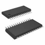 9DB433AGLFT
The activity of extra discounts on wholesale prices is in full swing…
Please fill in your contact information and we will send you the latest wholesale price list.






