 ChipApex | Global Electronic Components Supplier
9DB801BGLF
Search Product
Search Post
— IC芯片 | 连接器 | 传感器 | 被动器件 —
Search productSearch post
— IC芯片 | 连接器 | 传感器 | 被动器件 —
Consult the customer manager about the wholesale price.
consultation hotline:86-132-6715-2157
email:[email protected]
Contact the product manager for consultation. One-stop consultation is available.
Do you want a lower wholesale price? Please send us your inquiry and we will reply immediately.
The Renesas 9DB801BGLF is a clock buffer designed for PCI Express Gen1 applications. It features eight differential outputs and operates within a supply voltage range of 3.135V to 3.465V. The device supports a maximum frequency of 220MHz and utilizes a 48-TSSOP package with surface-mount installation. It includes an integrated Phase-Locked Loop (PLL) and supports differential input/output signaling. The component is rated for operation between 0°C and 70°C.
This component is listed as obsolete or not recommended for new designs by the manufacturer. Availability is limited to existing stock from distributors. Verification of RoHS compliance status and specific moisture sensitivity levels requires direct consultation with authorized suppliers or official datasheets prior to procurement.
Engineers should verify that the 220MHz bandwidth meets system requirements, as this model targets Gen1 specifications. For designs requiring higher throughput, such as PCIe Gen2 or Gen3, newer models like the 9DB803 series are recommended. Ensure the 48-TSSOP footprint matches the PCB layout constraints.
The 9DB801 belongs to the Renesas 9DB801 family of clock buffers. It shares functional similarities with other members like the 9DB801BGLFT but differs in packaging or termination options. This part serves as a legacy solution for older PCIe architectures where lower jitter and high fan-out were required.
The 9DB803DGLF is identified as a similar replacement option. Designers must evaluate differences in supported PCIe generations and electrical characteristics when substituting this obsolete part.
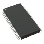 9DB801BGLF
The activity of extra discounts on wholesale prices is in full swing…
Please fill in your contact information and we will send you the latest wholesale price list.





